

Semiconductor device and semiconductor device manufacturing method
a semiconductor device and semiconductor technology, applied in the direction of semiconductor/solid-state device details, coatings, chemical vapor deposition coatings, etc., can solve the problem of not being able to sufficiently suppress the increase in leakage curren
- Summary
- Abstract
- Description
- Claims
- Application Information
AI Technical Summary
Benefits of technology
Problems solved by technology
Method used
Image

Examples
first embodiment
[0046] (First Embodiment)
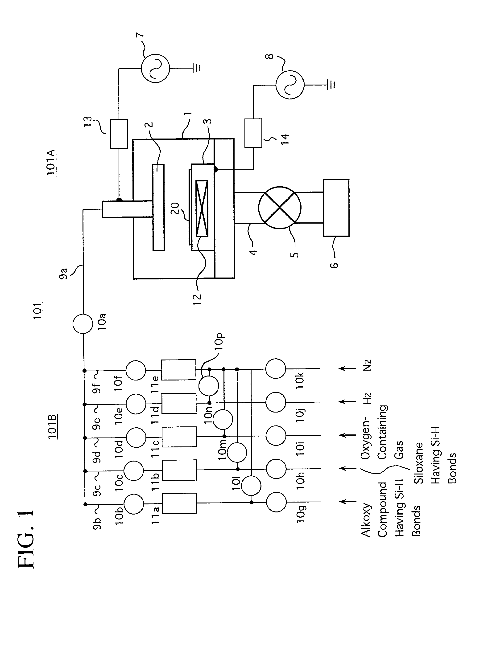
[0047] FIG. 1 is a side view showing a configuration of the parallel-plate type plasma CVD film forming equipment 101 employed in a film forming method according to an embodiment of the present invention.
[0048] This plasma CVD film forming equipment 101 comprises a film forming portion 101A that is the place at which a silicon-containing insulating film is formed by the plasma gas on a substrate 20, and a film forming gas supplying portion 101B having a plurality of gas supply sources constituting the film forming gas.
[0049] As shown in FIG. 1, the film forming portion 101A has a chamber 1 whose pressure can be reduced, and the chamber 1 is connected to an exhausting device 6 via an exhaust pipe 4. A switching valve 5 for controlling the open and the close between the chamber 1 and the exhausting device 6 is provided in the middle of the exhaust pipe 4. A pressure measuring means such as a vacuum gauge (not shown) for monitoring the pressure in the chamber 1...
second embodiment
[0062] (Second Embodiment)
[0063] The examination, made by the inventors of the present invention, about the silicon-containing insulating film, that is formed by the above plasma CVD equipment, will be explained hereunder.
[0064] First, the well-known parallel-plate type plasma CVD equipment is employed as the above plasma CVD equipment. The lower electrode 3 of the upper and lower electrodes 2, 3 is also used as a substrate holder, and the heater 12 for heating the substrate is built in the lower electrode 3.
[0065] (Formation of Samples)
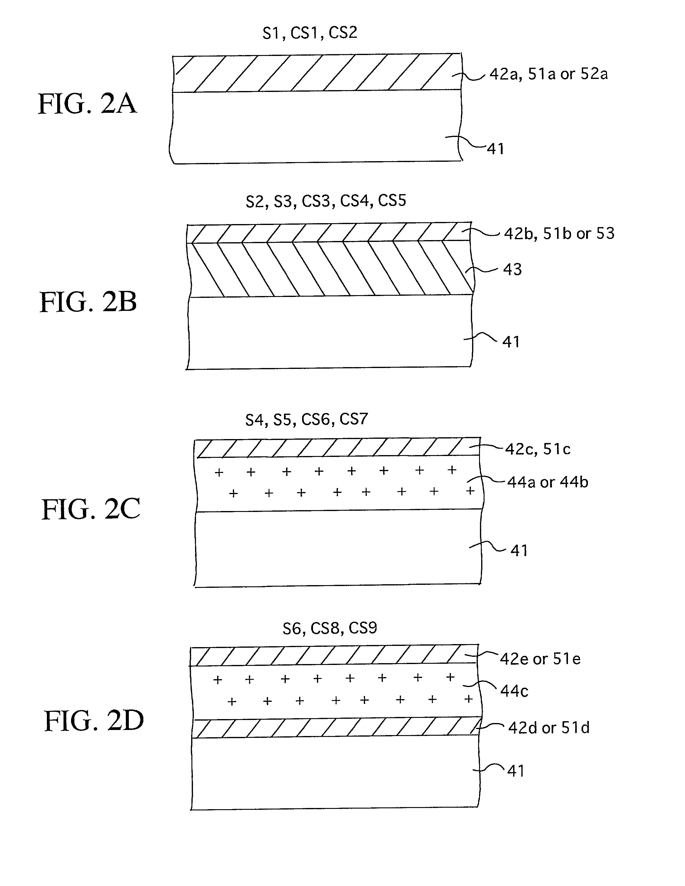
[0066] FIGS. 2A to 2E are sectional views showing samples having the silicon oxide film (a silicon-containing insulating film) of the present invention.
[0067] As shown in FIG. 2A, a sample S1 has a silicon oxide film (this means a silicon-containing insulating film, and referred to as a "PE-CVD TMS SiO.sub.2 film" hereinafter) 42a, that is formed by the PE-CVD method using the film forming gas containing trimethoxysilane (TMS) on a silicon substrate ...
third embodiment
[0157] (Third Embodiment)
[0158] Next, a semiconductor device manufacturing method according to a third embodiment of the present invention will be explained with reference to FIGS. 11A and 11B hereunder.
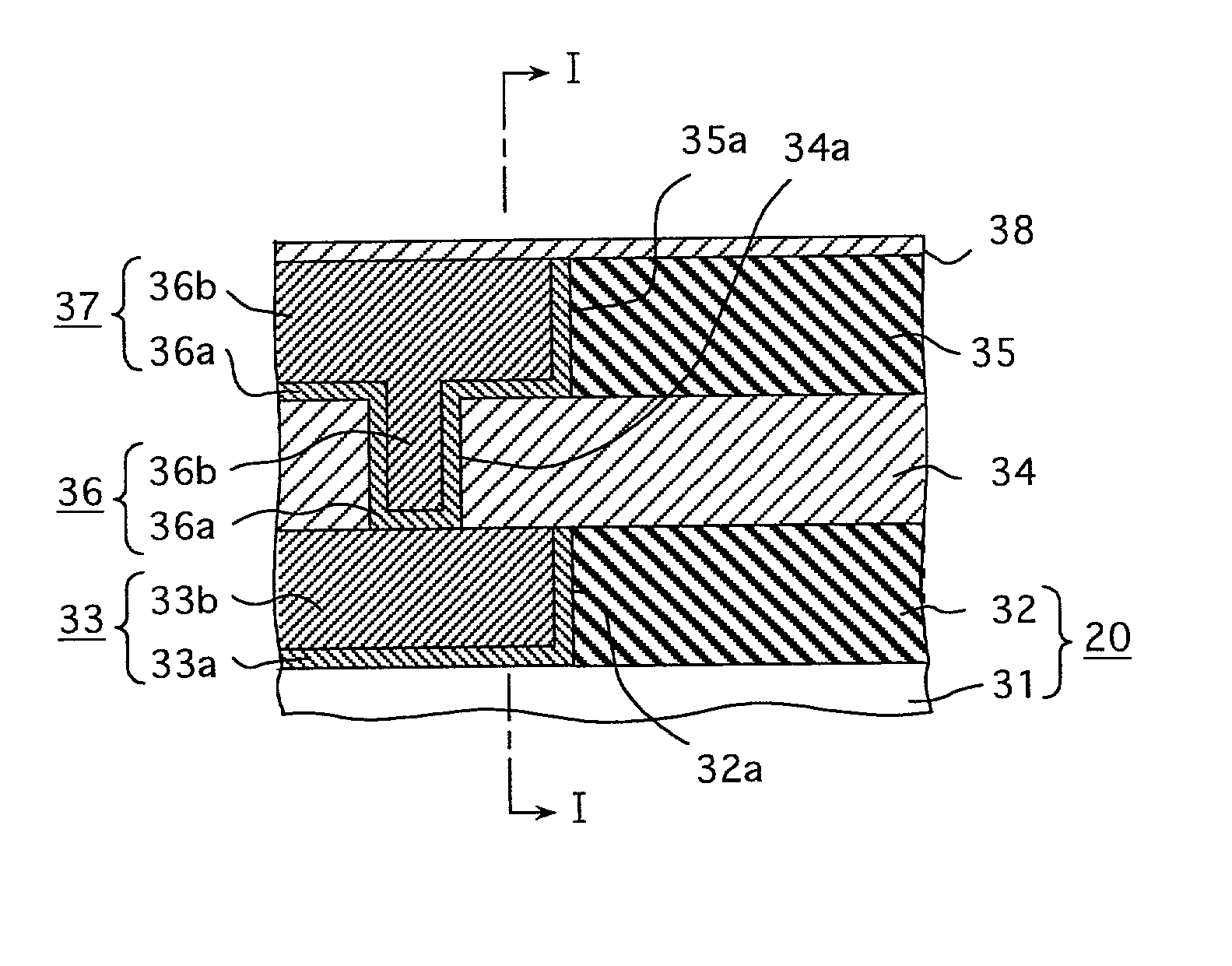
[0159] FIG. 11A is a sectional view showing a semiconductor device according to the third embodiment of the present invention. FIG. 11B is a sectional view taken along a I-I line in FIG. 11A.
[0160] This semiconductor device is formed of a lower wiring buried insulating film 32 made of an SiOF film with a thickness of approximately 1 m on a base substrate 31. a lower wiring recess 32a is formed in the lower wiring buried insulating film 32 and a lower wiring 33 is buried therein. Moreover, an inter-wiring layer insulating film (a protection layer) 34 made of a PE-CVD TMS SiO.sub.2 film (a silicon-containing insulating film) with a thickness of approximately 10 nm according to the present invention, and a upper wiring buried insulating film 35 made of an SiOF film with a thickness of a...
PUM
| Property | Measurement | Unit |
|---|---|---|
| Length | aaaaa | aaaaa |
| Frequency | aaaaa | aaaaa |
| Frequency | aaaaa | aaaaa |
Abstract
Description
Claims
Application Information