Chemistry for chemical vapor deposition of titanium containing films

a technology of titanium containing film and chemical vapor deposition, which is applied in the direction of chemical vapor deposition coating, coating, coating process of metallic materials, etc., can solve the problems of high deposition temperature, inability to fully perform the function of thin films, and increased likelihood of gaps

Inactive Publication Date: 2002-01-31
MICRON TECH INC
View PDF0 Cites 9 Cited by
  • Summary
  • Abstract
  • Description
  • Claims
  • Application Information

AI Technical Summary

Problems solved by technology

If these thin films are not deposited in a uniform manner, gaps may be created which prevent the thin film from fully performing its function.
The likelihood of the existence of these gaps tends to increase as the films become thinner.
The problem with this method is the extremely high deposition temperatures required.
First, high temperature may be incompatible with or even detrimental to other elements of the integrated circuit, and, second, excessive cycling from low to high temperatures can damage a circuit, thereby reducing the percentage of reliable circuits produced from a wafer.
The primary disadvantage of sputter deposition is that it results in films having poor step coverage, so it may not be widely useable in submicron processes.
Films deposited by sputter deposition on slanted or vertical surfaces do not exhibit uniform thickness, and the density of films deposited on these surfaces is usually not as high as the films deposited on horizontal surfaces.
The primary disadvantage of spin-on deposition is that nominal uniformity can only be achieved at relatively high thicknesses.
It is generally not useful for the deposition of thin films.
However, the hot wall reactor process is also characterized by low deposition rates, high temperatures, and the potential for the occurrence of unwanted reactions on the walls of the reaction chamber.
Conversely, the cold wall reactor exhibits high deposition rates but poor step coverage.
Exposure to extreme temperatures and excessive cycling from low to high temperatures during the fabrication of integrated circuits can render the circuits useless.
However, the current plasma deposition technology does have its limitations.
Because of the higher pressures associated with deposition in a cold wall reactor, it is difficult to deposit films that exhibit a high degree of uniform coverage in contacts and vias having high aspect ratios.
This difficulty extends to both the vertical surfaces of the contacts and vias as well as the horizontal surfaces at the base of the contacts and vias.

Method used


Image

  • Chemistry for chemical vapor deposition of titanium containing films
  • Chemistry for chemical vapor deposition of titanium containing films
  • Chemistry for chemical vapor deposition of titanium containing films

Examples


Embodiment Construction

[0031] In the interest of clarity, not all features of an actual implementation into an integrated circuit process are described in this specification. This illustration is restricted to those aspects of an integrated circuit process involving the deposition of thin films. Conventional details of integrated circuit processes, such as mask generation, resist casting, resist development, etching, doping, cleaning, implantation and annealing are not presented as such details are well known in the art of integrated circuit manufacture.

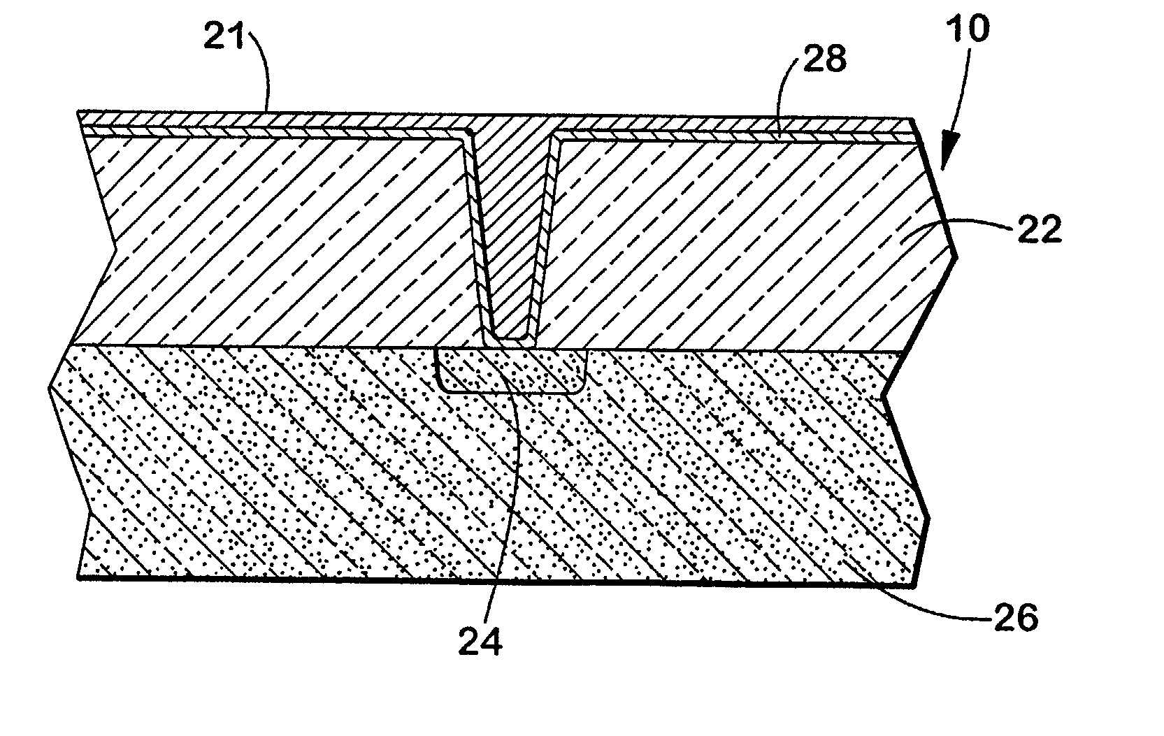
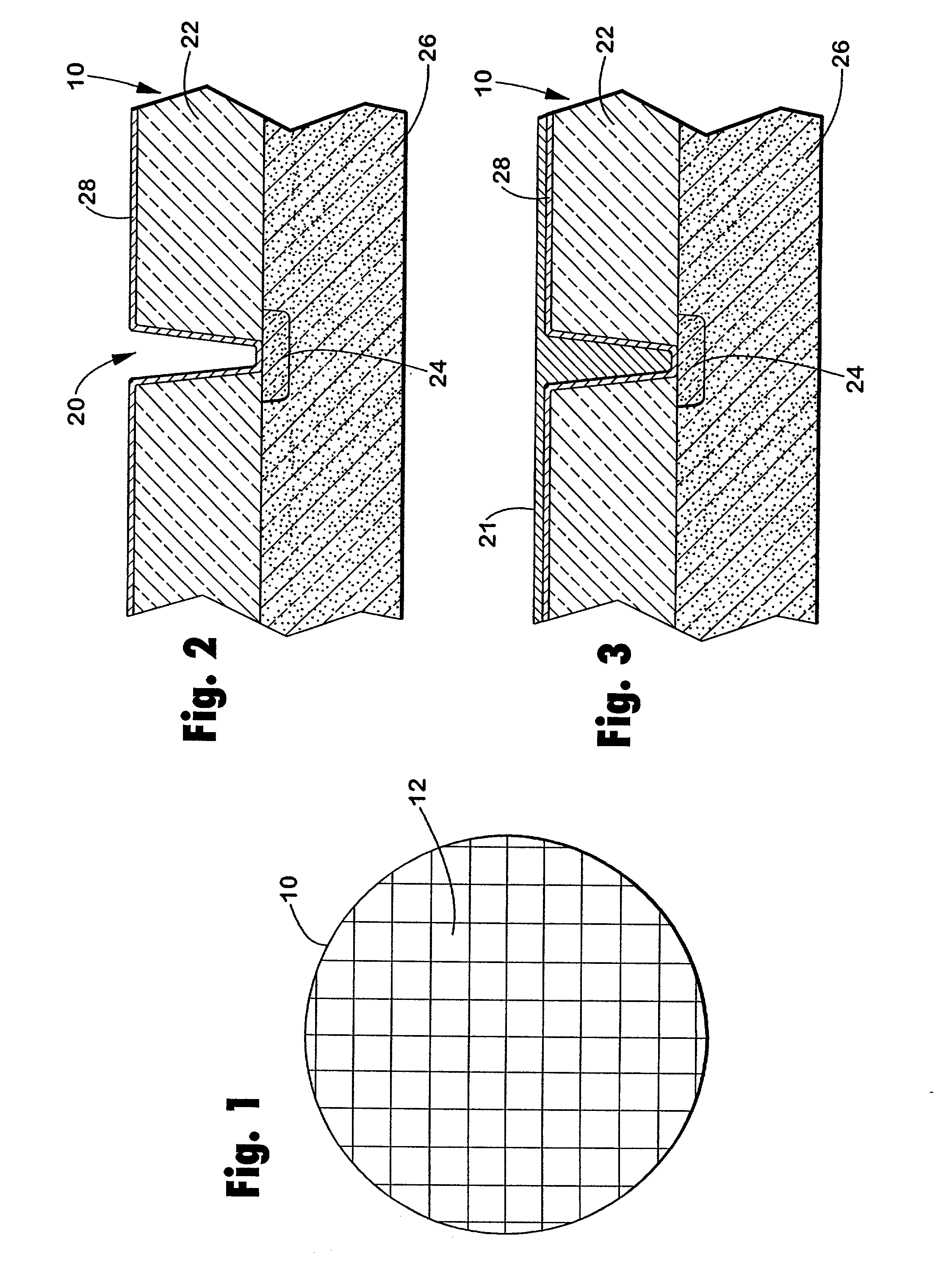
[0032] Turning now to the drawings, a typical semiconductor wafer is illustrated in FIG. 1 and designated by a reference numeral 10. The wafer 10 includes a number of different regions, known as die regions 12. Each die region 12 may include an integrated circuit containing various features and fabricated using various materials and processes. For the purposes of this discussion, one of the die regions 12 will be discussed. The die region 12 includes a thi...


PUM

PropertyMeasurementUnit
pressureaaaaaaaaaa
pressureaaaaaaaaaa
temperatureaaaaaaaaaa

Abstract

Titanium-containing films exhibiting excellent uniformity and step coverage are deposited on semiconductor wafers in a cold wall reactor which has been modified to discharge plasma into the reaction chamber. Titanium tetrabromide, titanium tetraiodide, or titanium tetrachloride, along with hydrogen, enter the reaction chamber and come in contact with a heated semiconductor wafer, thereby depositing a thin titanium-containing film on the wafer's surface. Step coverage and deposition rate are enhanced by the presence of the plasma. The use of titanium tetrabromide or titanium tetraiodide instead of titanium tetrachloride also increases the deposition rate and allows for a lower reaction temperature. Titanium silicide and titanium nitride can also be deposited by this method by varying the gas incorporated with the titanium precursors.

Description

[0001] 1. Field Of The Invention[0002] The present invention relates generally to the field of integrated circuit manufacturing technology and, more particularly, to an improved method for depositing thin films.[0003] 2. Background Of The Related Art[0004] In the manufacturing of integrated circuits, numerous microelectronic circuits are simultaneously manufactured on semiconductor substrates. These substrates are usually referred to as wafers. A typical wafer is comprised of a number of different regions, known as die regions. When fabrication is complete, the wafer is cut along these die regions to form individual die. Each die contains at least one microelectronic circuit, which is typically replicated on each die. One example of a microelectronic circuit which can be fabricated in this way is a dynamic random access memory ("DRAM").[0005] Although referred to as semiconductor devices, integrated circuits are in fact fabricated from numerous materials of varying electrical proper...

Claims


Application Information

Patent Timeline
Patent Type & Authority Applications(United States)
IPC IPC(8): C23C16/14C23C16/34C23C16/42H01L21/285H01L21/768
CPCC23C16/14C23C16/34C23C16/42H01L21/28568H01L21/76843
Inventor SHARAN, SUJITRHODES, HOWARD E.IRELAND, PHILIP J.SANDHU, GURTEJ S.
Owner MICRON TECH INC
Why Eureka
Try Eureka