Semiconductor device

a technology of semiconductors and devices, applied in the direction of semiconductor devices, basic electric elements, electrical equipment, etc., can solve the problems of depletion capacitance and low breakdown voltag

Inactive Publication Date: 2002-02-14
INST OF MICROELECTRONICS CHINESE ACAD OF SCI
View PDF0 Cites 19 Cited by
  • Summary
  • Abstract
  • Description
  • Claims
  • Application Information

AI Technical Summary

Benefits of technology

[0004] It is an object of the present invention also to provide a semiconductor device which is efficient and reliable for application as a radio frequency power device and which is capable of achieving one or more of a low parasitic feedback capacitance, a high breakdown voltage, a low channel resistance and a high transconductance in a controllable manner.
[0006] In accordance with an exemplary embodiment of the invention which will be described hereafter in detail, a VDMOSFET device has spaced apart sources on one face and a drain on the opposite face of a semiconductor body. Between the spaced apart sources there are provided spaced apart gate structures, and between the spaced apart gate structures there is provided an additional electrode which, in operate of the device, is connected to source. The split gate structure achieves a reduced gate overlap capacitance, just as in the prior art proposal hereinbefore described, and the additional electrode effects depletion of the underlying part of the semiconductor body and reduces the C.sub.SI component of the feedback capacitance. With a reduced C.sub.OX and a reduced C.sub.SI, the feedback capacitance C.sub.rss is much reduced and the high frequency capability of the device correspondingly enhanced.
[0007] In addition to exhibiting an enhanced high frequency capability, an additional advantageous effect is achieved by the invention in that the high electric fields caused by current crowding in the prior art split gate device are significantly reduced so that the device exhibits improved voltage breakdown levels.
[0008] The feedback capacitance C.sub.rss of the hereinafter described embodiment is also relatively strongly dependent on bias conditions which is significant in regard to improving the efficiency, power gain and output power of the device.

Problems solved by technology

However, the modified split gate structure gives rise to two drawbacks, namely: (1) the split gate structure suffers from a lower breakdown voltage due to high electric field crowding on the substrate surface under the gate ends, and (2) the substrate depletion capacitance (C.sub.SI) between gate and drain is large, because there is less depletion in the substrate.

Method used


Image

  • Semiconductor device
  • Semiconductor device
  • Semiconductor device

Examples


Embodiment Construction

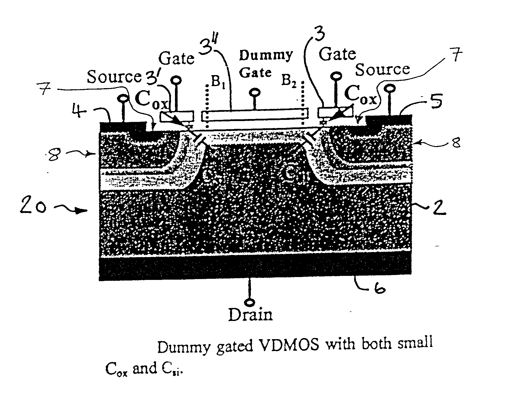
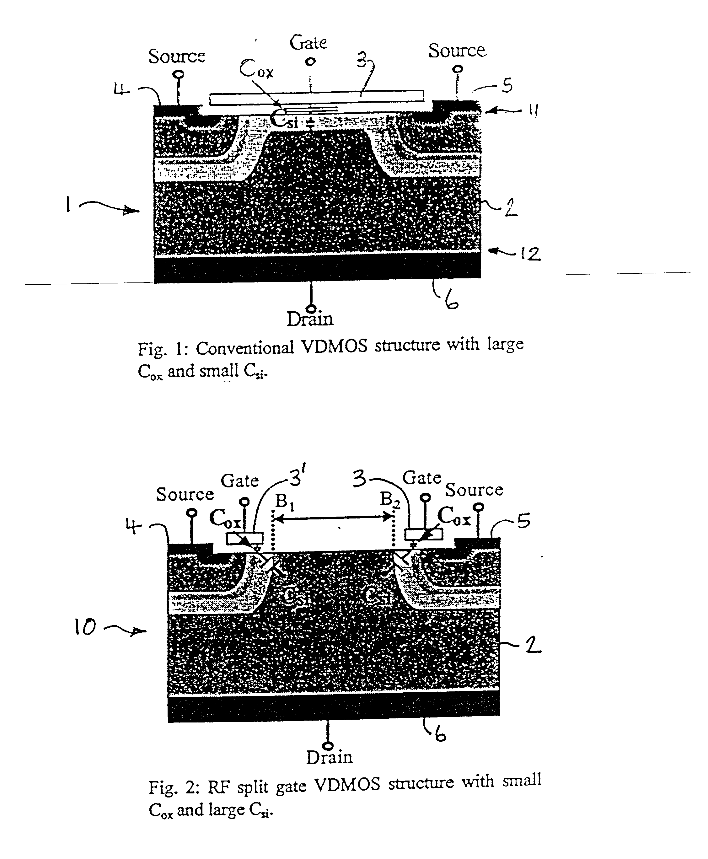
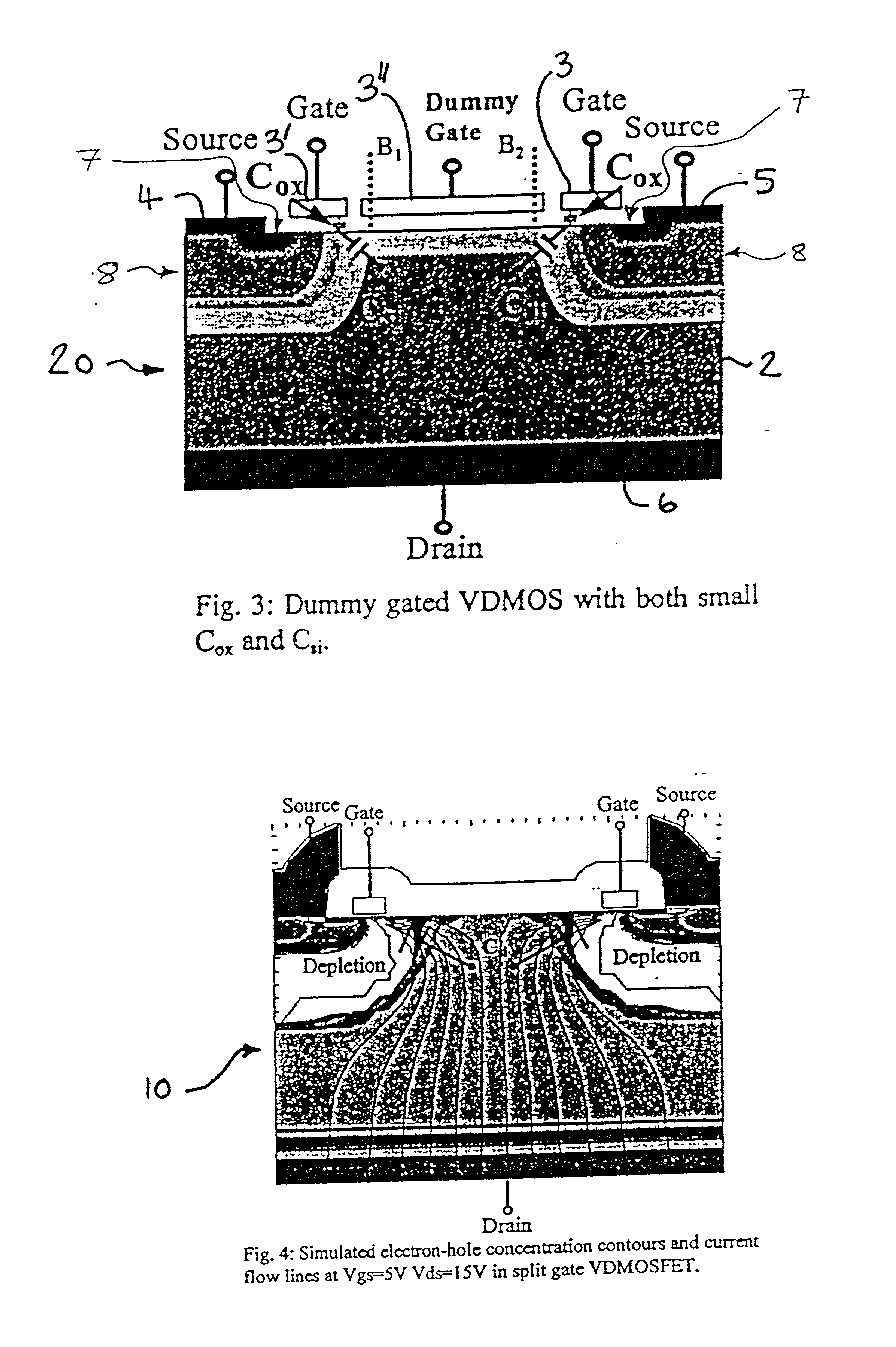
[0022] A conventional VDMOS structure, as originally proposed and as well known, is schematically illustrated in FIG. 1. As shown, the device generally indicated by 1, comprises an N- silicon semiconductor body 2, having a unitary gate 3 and two spaced-apart sources 4, 5 at its upper surface 11 and a drain 6 at its lower surface 12. The sources 4, 5 couple to respective N+ regions 7 located within P- type bodies 8 formed in the N- silicon body which is an epitaxial layer formed on an N+ substrate. As is also well known in the art, the amount of capacitive coupling between the gate and the drain limits the high frequency capability of the device such that that the device of FIG. 1 operates at a lower frequency capability than conventional RF LDMOSFET devices. The high frequency capability of a VDMOS device is a function of its feedback capacitance (C.sub.rss) which, in turn, depends upon two factors, namely the gate-substrate overlap capacitance (C.sub.OX) and the silicon substrate d...


PUM


Abstract

A VD (vertical diffusion) MOSFET device for use in RF power applications has a split gate structure and an additional, dummy gate is provided between the spaced apart gates and, in operation of the device, is electrically coupled to source electrodes provided outside of the gates. The split gate structure reduces gate overlap capacitance and the dummy gate induces depletion in the semiconductor body of the device and reduces the substrate capacitance. The gate overlap capacitance and the substrate capacitance both contribute to the feedback capacitance of the device which has to be as low as possible for high frequency operation. By reducing both of these components, the invention provides advantageous high frequency operation.

Description

[0001] This invention relates to a semiconductor device and more particularly, but not exclusively, concerns a VD (vertical diffusion) MOS device for use in RF (radio frequency) power applications for example.[0002] A particular kind of semiconductor device, known in the art as a VDMOSFET, has been identified as being particularly useful for broadband radio frequency (RF) applications due to its high reliability and due to the existence of well tried and tested fabrication technology appropriate to its manufacture (see H. Esaki and O. Ishikawa, "A 900 MKz, VD-MOSFET with silicide gate self-aligned channel", International Electron Devices Meeting Digest, Abstract 16.6 pp.447-449 (1984)). VD MOS devices dominate high power RF applications thanks to their high voltage capability. As compared to RF LD (lateral diffusion) MOSFETs, which are used in high frequency, narrow band applications where higher gain is needed, VDMOSFET devices are however known to exhibit a lower frequency capabil...

Claims


Application Information

Patent Timeline
Patent Type & Authority Applications(United States)
IPC IPC(8): H01L29/06H01L29/423H01L29/78
CPCH01L29/402H01L29/42376H01L29/7802
Inventor XU, SHUMINGFOO, PANG DOW
Owner INST OF MICROELECTRONICS CHINESE ACAD OF SCI
Why Eureka
Try Eureka