Thin layer semi-conductor structure comprising a heat distribution layer

a thin layer, semi-conductor technology, applied in the direction of transistors, electric devices, solid-state devices, etc., can solve the problems of high cost, need to resort to non-standard micro-electronic equipment, and the drawback of silica, so as to reduce the thickness of the first substrate

Inactive Publication Date: 2002-07-11
JOLY JEAN PIERRE +2
View PDF0 Cites 50 Cited by
  • Summary
  • Abstract
  • Description
  • Claims
  • Application Information

AI Technical Summary

Benefits of technology

0024] Making said semi-conductor surface layer may include reducing the thickness of the first substrate.

Problems solved by technology

The major drawback of this technology is its cost due to the high dose ion implantation, and the need to resort to non standard micro-electronic equipment.
Silica has however one great drawback: its very low thermal conductivity which is of the order of 0.2 W.m.sup.-1.K.sup.-1.
This causes a substantial transitory and localised temperature rise, altogether problematic for the proper operation of the components.
However, the drawbacks of this reduction in thickness are that on the one hand stray capacitance is increased (thereby reducing the rapidity of the components) and, on the other hand, electrical strength is reduced.
Furthermore, the reduction in thickness of the insulating layer is not easy to obtain in the implementation of processes of the molecular adhesion type where a good quality of adhesion is obtained much more easily with layers of thickness exceeding 300 nm.
The materials proposed (for example diamond) do not have a good interface with silicon from the electrical point of view.
These solutions are certainly effective from the thermal point of view, but they are not easily applicable in association with the technologies of bonding by molecular adhesion.
It is indeed extremely difficult to bond materials of high thermal conductivity as conceived.
Because of this, heat dissipation in the component is substantial and the thermal conductivity of the silicon and / or of the dielectrics used is insufficient to provide a junction temperature which is not crippling.

Method used


Image

  • Thin layer semi-conductor structure comprising a heat distribution layer
  • Thin layer semi-conductor structure comprising a heat distribution layer
  • Thin layer semi-conductor structure comprising a heat distribution layer

Examples


Embodiment Construction

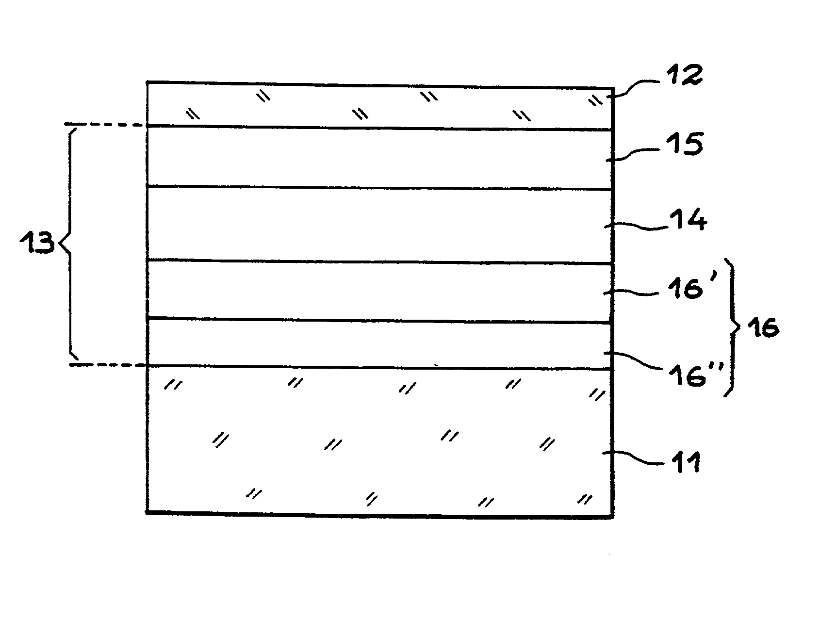
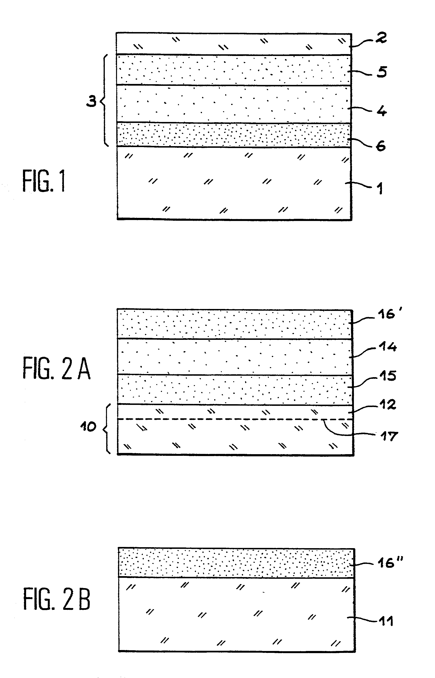
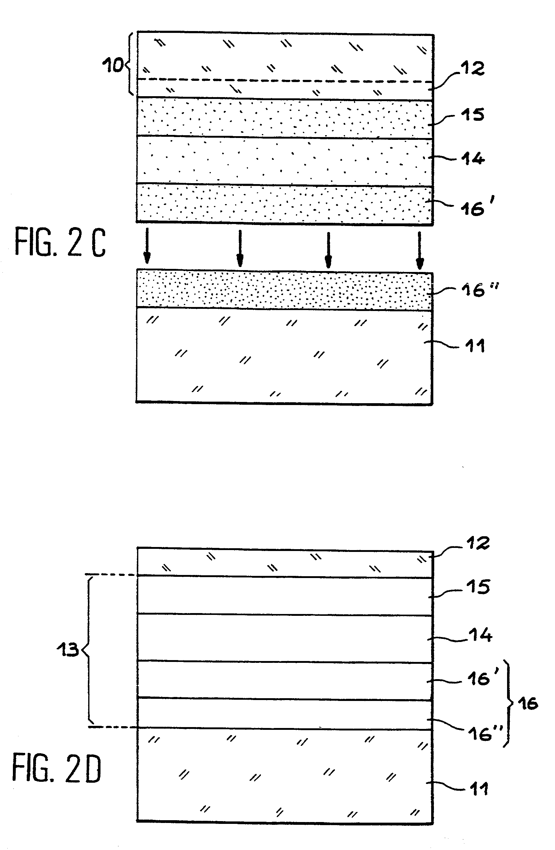
[0032] FIG. 1 shows a first example of a semi-conductor structure according to the invention. This structure comprises a support substrate 1 for example of silicon, a surface layer 2 of silicon and an intermediate zone 3. The intermediate zone 3 comprises at least one layer 4 of good thermal conductivity, an insulating layer 5 conferring good electrical quality of interface with the semi-conductor surface layer 2 and an insulating layer 6, being able to be of low thermal conductivity, adhering to the support substrate 1.

[0033] In the case of an SOI structure implementing the molecular adhesion process, the layer 6 may in particular be made of silica. This layer 6 may of course be a multi-layer.

[0034] When the layer 4 of good thermal conductivity makes it possible to have directly a good electrical interface with the surface layer of silicon 2, the layer 5 may be omitted.

[0035] The structure according to the invention makes it possible to retain the materials and thicknesses allowing...


PUM

PropertyMeasurementUnit
thicknessesaaaaaaaaaa
thermal conductivityaaaaaaaaaa

Abstract

The invention concerns a thin layer semi-conductor structure including a semi-conductor surface layer (2) separated from a support substrate (1) by an intermediate zone (3), the intermediate zone (3) being a multi-layer electrically insulating the semi-conductor surface layer from the support substrate. The intermediate zone has a considered sufficiently good electrical quality of interface with the semi-conductor surface layer and includes at least one first layer, of satisfactory thermal conductivity to provide a considered as correct operation of the electronic device or devices which are to be elaborated from the semi-conductor surface layer (2), the intermediate zone including additionally a second insulating layer of low dielectric constant, located between the first layer and the support substrate.

Description

[0001] The present invention concerns a thin layer semi-conductor structure and processes for embodying such a structure.[0002] By thin layer semi-conductor structure is understood a structure having on the surface a fine semi-conductor layer in which will be manufactured electronic devices (this layer is called an active layer) and a substrate performing a mechanical support role. This substrate is generally electrically insulated form the surface layer. The substrate is constituted either from a solid insulating material (a dielectric in the case of the SOS), or from a conductor or semi-conductor material. In this latter case, it may be of the same material as that of the surface layer (the case of SOI), generally insulated form the surface layer by an insulation layer. In the case of the SOI, the mechanical substrate is usually constituted by a silicon substrate with a layer of silica on the surface, but it may also be constituted by a solid substrate of fused silica (silicon on ...

Claims


Application Information

Patent Timeline
Patent Type & Authority Applications(United States)
IPC IPC(8): H01L21/762H01L23/373
CPCH01L21/76251H01L23/3735H01L2924/0002H01L2924/00
Inventor JOLY, JEAN-PIERREBRUEL, MICHELJAUSSAUD, CLAUDE
Owner JOLY JEAN PIERRE
Why Eureka
Try Eureka