Method for fabricating metal interconnections

a metal interconnection and metal technology, applied in the direction of identification means, instruments, semiconductor devices, etc., can solve the problems of large delay of driving signals, process increase, cost increase, etc., and achieve low resistance interconnection, low resistance, and low price

Inactive Publication Date: 2002-09-12
SHARP KK
View PDF0 Cites 32 Cited by
  • Summary
  • Abstract
  • Description
  • Claims
  • Application Information

AI Technical Summary

Benefits of technology

0034] According to this embodiment, inexpensive low-resistivity interconnections which are stable even with large current density can b

Problems solved by technology

As a result of this, delay of driving signals would come up as a large problem.
According to this literature, it is pointed out that because a Cu film deposited by sputtering process is poor in adhesion to the ground glass substrate, a ground metal film of Ta or the like needs to be interveniently provided between the ground glass substrate and the Cu film in order to enhance the adhesion to the ground glass substrate.
However, in th

Method used


Image

  • Method for fabricating metal interconnections
  • Method for fabricating metal interconnections
  • Method for fabricating metal interconnections

Examples


embodiment 1

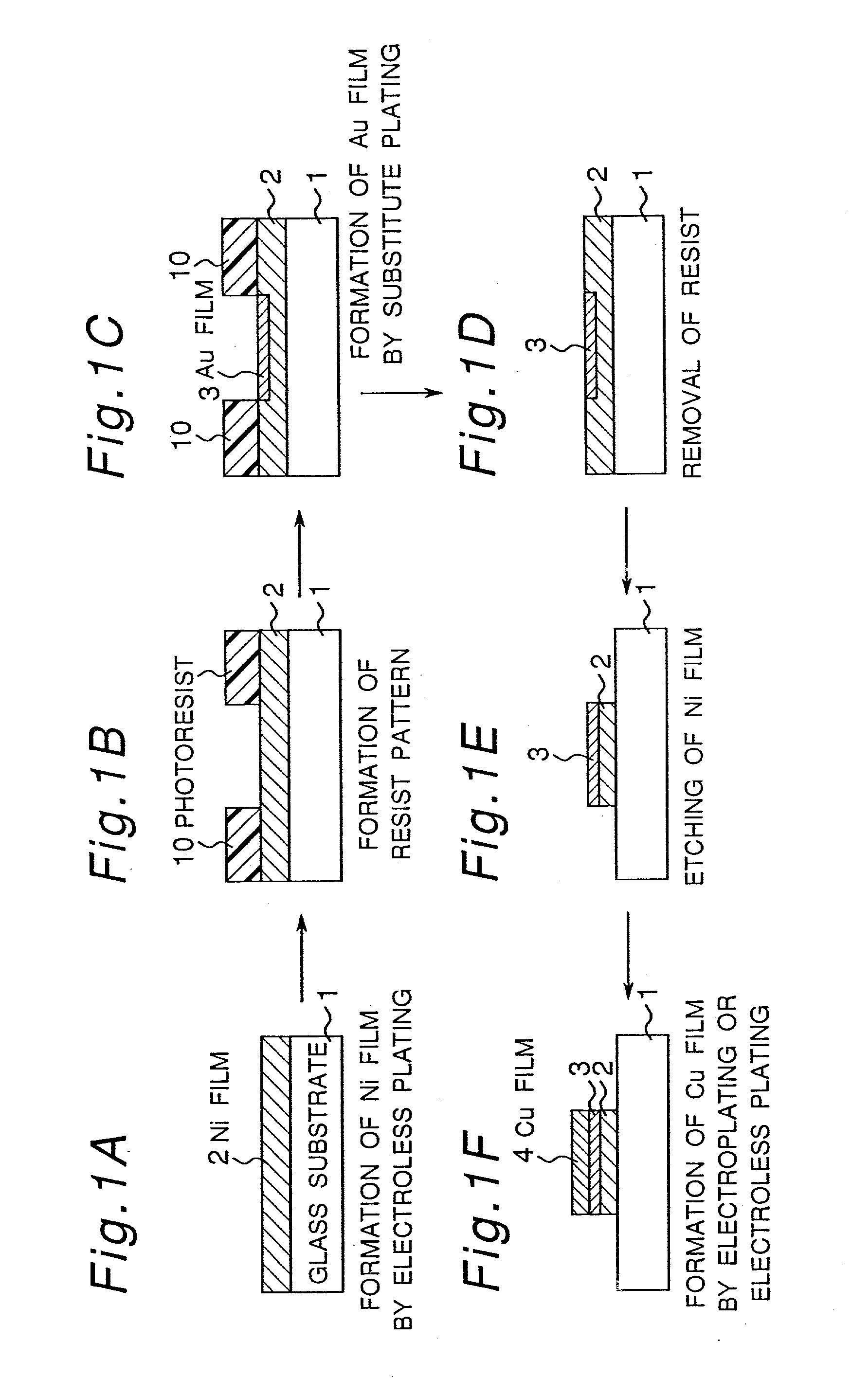
[0043] (Embodiment 1)

[0044] Embodiment 1 of the invention is constituted of first to sixth steps shown FIGS. 1A-1F, respectively.

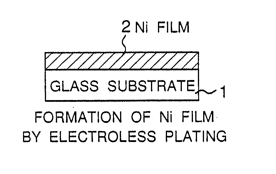
[0045] At the first step shown in FIG. 1A, on a glass substrate 1 as an insulating substrate, is formed a nickel (Ni) film 2 as a ground metal film superior in adhesion to glass by electroless plating.

[0046] More specifically, at this first step, the glass substrate (e.g., #1737 made by Corning Inc.) 1 having a thickness of, for example, 0.7 mm is degreased and cleaned by alkali or acid or organic solvent so that dirties of surfaces of the glass substrate 1 are removed. In this process, by using ultrasonic cleaning in combination, dirties are removed efficiently. Next, the glass substrate 1 is dipped into the aqueous solution containing amino compounds, by which coating of amino compounds is formed on the surface of the glass substrate 1. This coating of amino compounds is extremely high in adhesion to the glass substrate 1 and has amino groups, so that pa...

embodiment 2

[0083] (Embodiment 2)

[0084] Embodiment 2 is another fabrication method for obtaining interconnections of the same structure as the metal interconnections described in Embodiment 1.

[0085] FIGS. 3A-3F show first to sixth steps of Embodiment 2, respectively. The first to third steps of Embodiment 2 shown in FIGS. 3A-3C are the same as the first to third steps of Embodiment 1 shown FIGS. 1A-1C, respectively.

[0086] In detail, at the first step shown in FIG. 3A, on a glass substrate 11 which is an insulating substrate, is formed a nickel film 12 as a ground metal film superior in adhesion to glass by electroless plating. At the second step shown in FIG. 3B, a photoresist film 20 is formed on the Ni film 12 in correspondence to interconnecting portions. Then, at the third step shown in FIG. 3C, a Au film 13 which is a noble metal film is formed by electroless plating at an opening portion of the photoresist film 20, i.e., on the exposed Ni film 12. As in Embodiment 1, the thickness of the ...

embodiment 3

[0094] (Embodiment 3)

[0095] Embodiment 3 is another method for obtaining interconnections of the same structure as the metal interconnections described in Embodiment 1.

[0096] FIGS. 5A-5F show first to sixth steps of Embodiment 2, respectively.

[0097] In detail, at the first step shown in FIG. 5A, on a glass substrate 31 which is an insulating substrate, is formed a nickel film 32 as a ground metal film superior in adhesion to glass by electroless plating. The method of electroless Ni-plating, the thickness of the Ni film and the like are the same as in foregoing Embodiment 1. At the second step shown in FIG. 5B, a photoresist film 30 is formed on the Ni film 32 in correspondence to interconnecting portions. The method of forming the photoresist film 30 is the same as in foregoing Embodiment 1. However, in this embodiment, a patterned photoresist film 30 is formed in a region corresponding to the interconnecting portion. Then, at the third step shown in FIG. 5C, an opening portion of ...


PUM


Abstract

In the present method for fabricating metal interconnections, a Ni film is deposited on an insulating substrate by electroless plating, and a photoresist film is formed in a specified pattern on the Ni film. An Au film is deposited by electroless plating in a region where the Ni film is exposed and where the resist is not formed. The photoresist film is removed, and the Ni film exposed by the removal of the photoresist film is removed by etching. A Cu film is formed on the Au film by electroplating or electroless plating selectively. This method consists of only wet deposition process, involves less etching process and provides metal interconnections of low resistance.

Description

BACKGROUND OF THE INVENTION[0001] The present invention relates to a method for fabricating metal interconnections used for flat panel displays such as liquid crystal displays (LCD), plasma display panels (PDP), electrochromic displays (ECD) and electroluminescent displays (ELD), or flat panel sensors such as X-ray imaging devices.[0002] In a flat panel display typified by LCD, normally, display material such as liquid crystals or discharge gas is sandwiched between a pair of insulating substrates, and electrical interconnection lines are arrayed on at least one of the insulating substrates, where a voltage is applied to the display material via the electrical lines.[0003] For example, in the case of an active matrix drive type LCD, a plurality of gate electrodes and a plurality of data electrodes are provided in a matrix shape on an active matrix substrate, which is one of the pair of insulating substrates between which the display material is sandwiched. At intersections of these ...

Claims


Application Information

Patent Timeline
IPC IPC(8): G02F1/1343G09F9/30H01L21/288H01L21/3205H01L21/44H01L21/4763H01L21/768H01L29/49H01L29/786
CPCH01L29/4908H01L21/76838G02F1/136295G02F1/1345
Inventor IZUMI, YOSHIHIROCHIKAMA, YOSHIMASA
Owner SHARP KK
Why Eureka
Try Eureka