Compound semiconductor device and method of manufacturing the same
a technology of compound semiconductor and semiconductor substrate, which is applied in the direction of solid-state devices, transistors, capacitors, etc., can solve the problems of crystal defect generation and achieve the effect of preventing leakage current and preventing the generation of crystal defects in the compound semiconductor substra
- Summary
- Abstract
- Description
- Claims
- Application Information
AI Technical Summary
Benefits of technology
Problems solved by technology
Method used
Image
Examples
first embodiment
[0026] (First Embodiment)
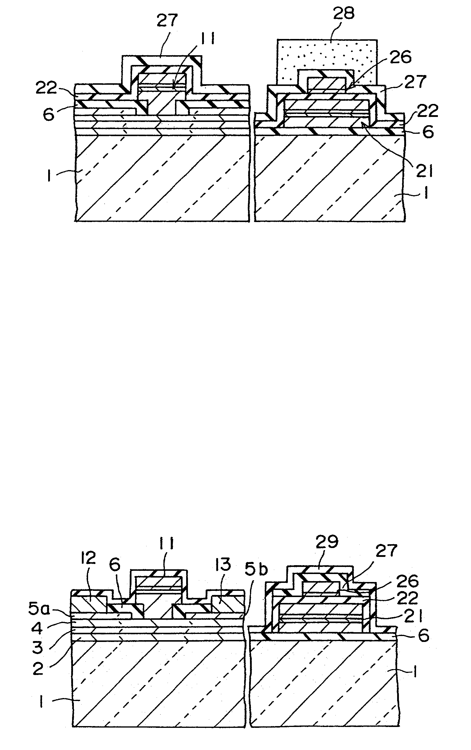
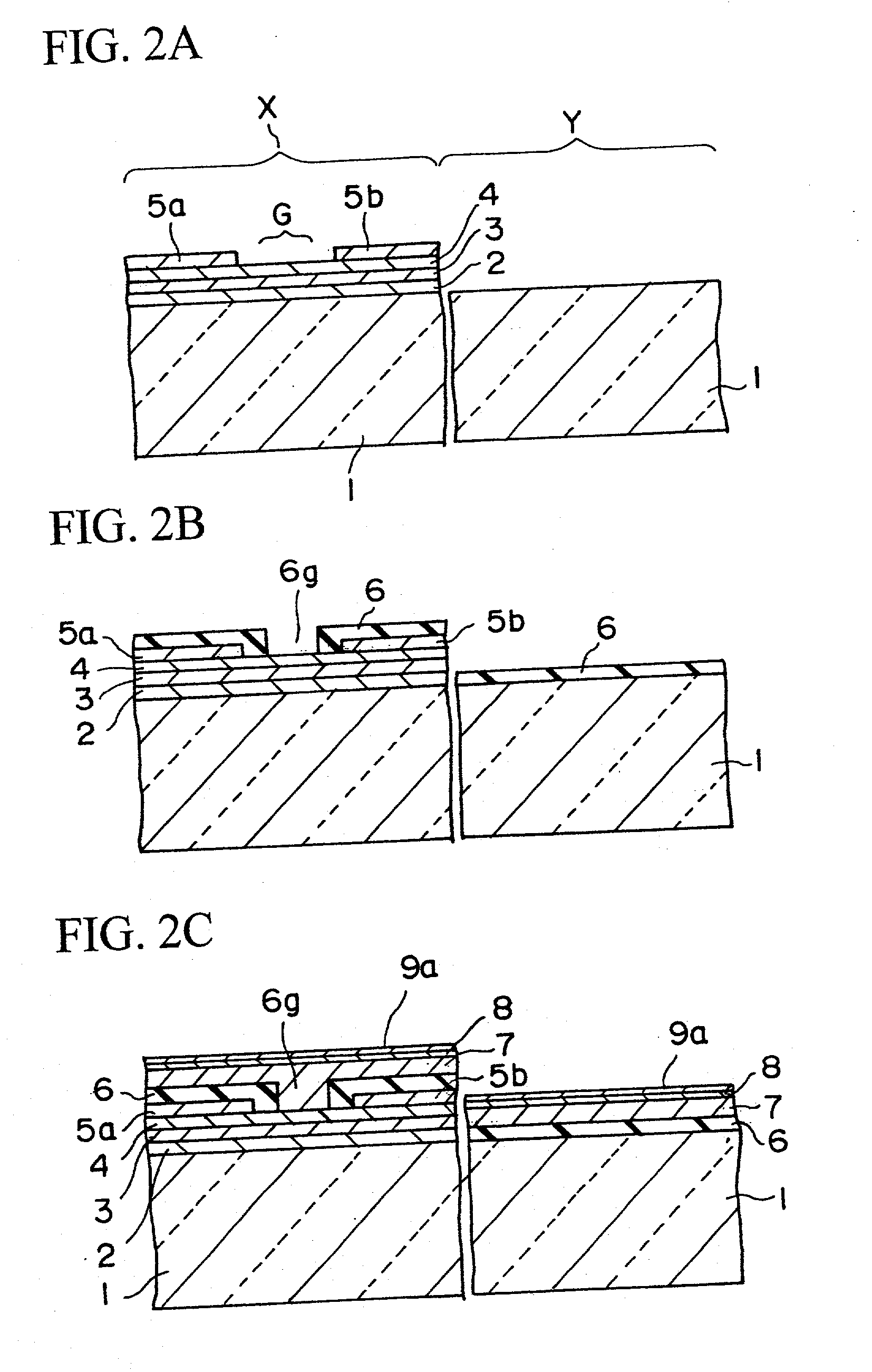
[0027] FIGS. 2A to 2K are showing steps of manufacturing a compound semiconductor device according to a first embodiment of the present invention.
[0028] First, as shown in FIG. 2A, a channel layer 2 formed of undoped InGaAs, a carrier supplying layer 3 formed of n.sup.+ type AlGaAs, and a Schottky layer 4 formed of undoped AlGaAs are formed in sequence on a transistor forming region of a compound semiconductor substrate 1 formed of semi-insulating GaAs. Then, cap layers 5a, 5b formed of n.sup.+ type GaAs are formed in a source region and a drain region of the Schottky layer 4 respectively. A gate electrode forming region G is assured between the source region and the drain region. As the n type impurity contained in the carrier supplying layer 3, the cap layers 5a, 5b, etc., for example, there is silicon which is doped by silane.
[0029] Under this condition, as shown in FIG. 2B, a first insulating film 6 is formed on two cap layers 5a, 5b, the Schottky layer ...
second embodiment
[0055] (Second Embodiment)
[0056] In the above first embodiment, a configuration in which a part of the first electrode 21 is covered with the dielectric film 22 is employed. Similarly, a capacitor structure in which the whole first electrode 21 is covered with the dielectric film 22 may be employed.
[0057] The steps of manufacturing such capacitor will be explained hereunder.
[0058] First, as shown in FIG. 2I, the second insulating film 27 is formed, and then the region covered with the resist 28 is expanded up to the first electrode 21 and its peripheral region, as shown in FIG. 6A.
[0059] Then, as shown in FIG. 6B, when the second insulating film 27 and the dielectric film 22 are etched using the resist 28 as a mask, the entire first electrode 21 is covered with the second insulating film 27 and the dielectric film 22. In this case, since the second insulating film 27 and the dielectric film 22 are removed from the transistor forming region X, there is no possibility of applying the ...
PUM
 Abstract
Description
Claims
Application Information


