ESD protection circuit with very low input capacitance for high-frequency I/O ports

a protection circuit and high-frequency technology, applied in the direction of semiconductor devices, semiconductor/solid-state device details, diodes, etc., can solve the problems of large loading to the i/o port, reducing the response speed of the i/o port at high frequencies, and the gate oxide layer of metal-oxide-semiconductor transistors (mos) becomes thinner and more easily damaged by unexpected stress, etc., to achieve the effect of reducing the chip area required by th

Inactive Publication Date: 2002-09-19
TAIWAN SEMICON MFG CO LTD
View PDF2 Cites 156 Cited by
  • Summary
  • Abstract
  • Description
  • Claims
  • Application Information

AI Technical Summary

Benefits of technology

0019] Another advantage of the present invention is that the diodes are forward-biased to release ESD stress, unlike the prior art, which is reverse-biased to release ESD stress. Thus, each diode can be constructed as a smaller sized element. The chip area required by the I/O port can be reduced and, as a result, the input capacitance is further reduced.
0020] The present invention also provides a power-rail ESD clamp circuit, suitable for an integrated circuit, coupled between two power lines. The ESD clamp circuit between power lines includes a substrate-triggered NMOS and an ESD detection circuit. The N

Problems solved by technology

As the manufacturing process for integrated circuit (IC) improves, the gate oxide layer of metal-oxide-semiconductor transistors (MOS) becomes thinner and more easily damaged by unexpected stress.
However, large elements will cause large loading to the I/O port. FIG. 5 is the equivalent circuit of FIG. 1(a), showing parasitic capacitors therein.
Such high input capacitance will lower the response speed of the I/O port at high frequencies.
Thus, circuit designs as shown in FIG. 1(a) or FIG. 1(b) are not suitable for high-frequency or high-s

Method used


Image

  • ESD protection circuit with very low input capacitance for high-frequency I/O ports
  • ESD protection circuit with very low input capacitance for high-frequency I/O ports
  • ESD protection circuit with very low input capacitance for high-frequency I/O ports

Examples


Embodiment Construction

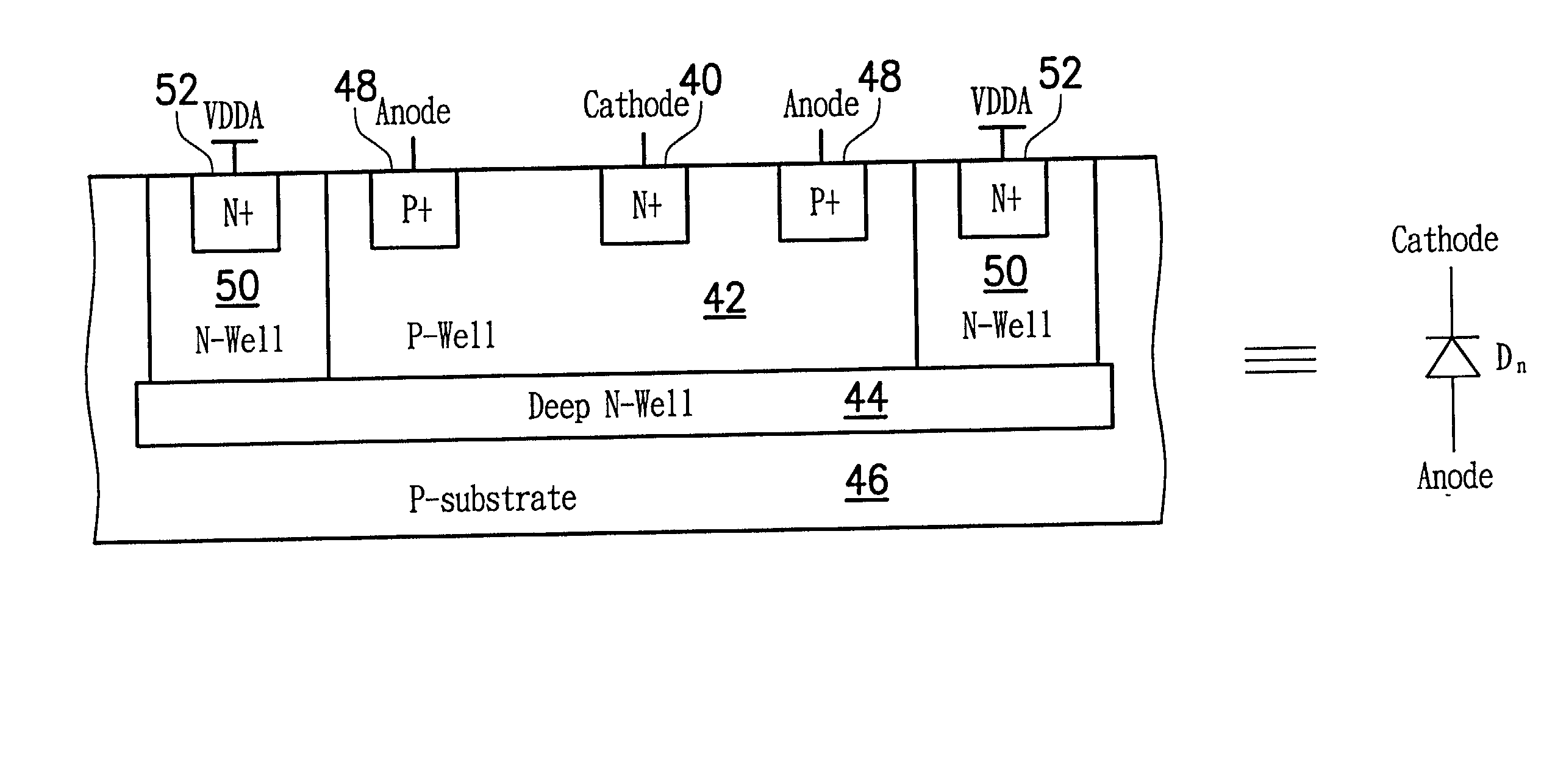
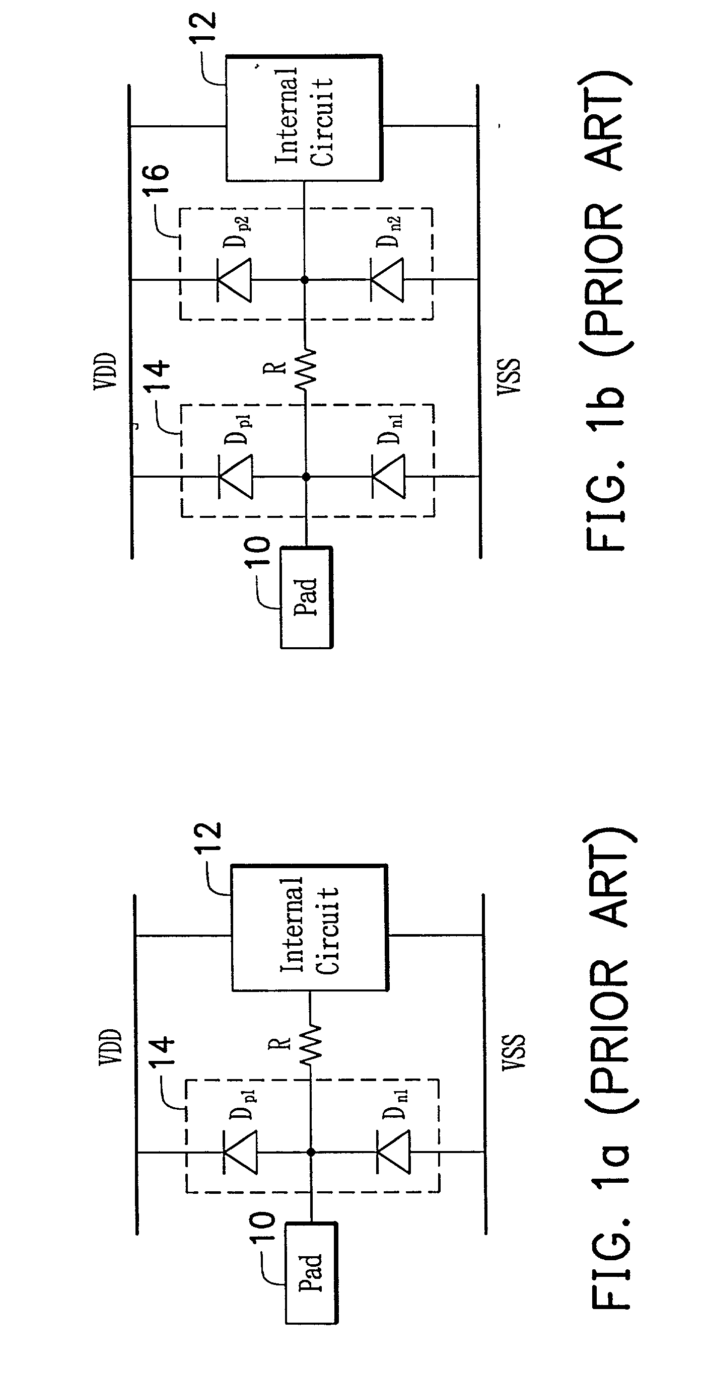
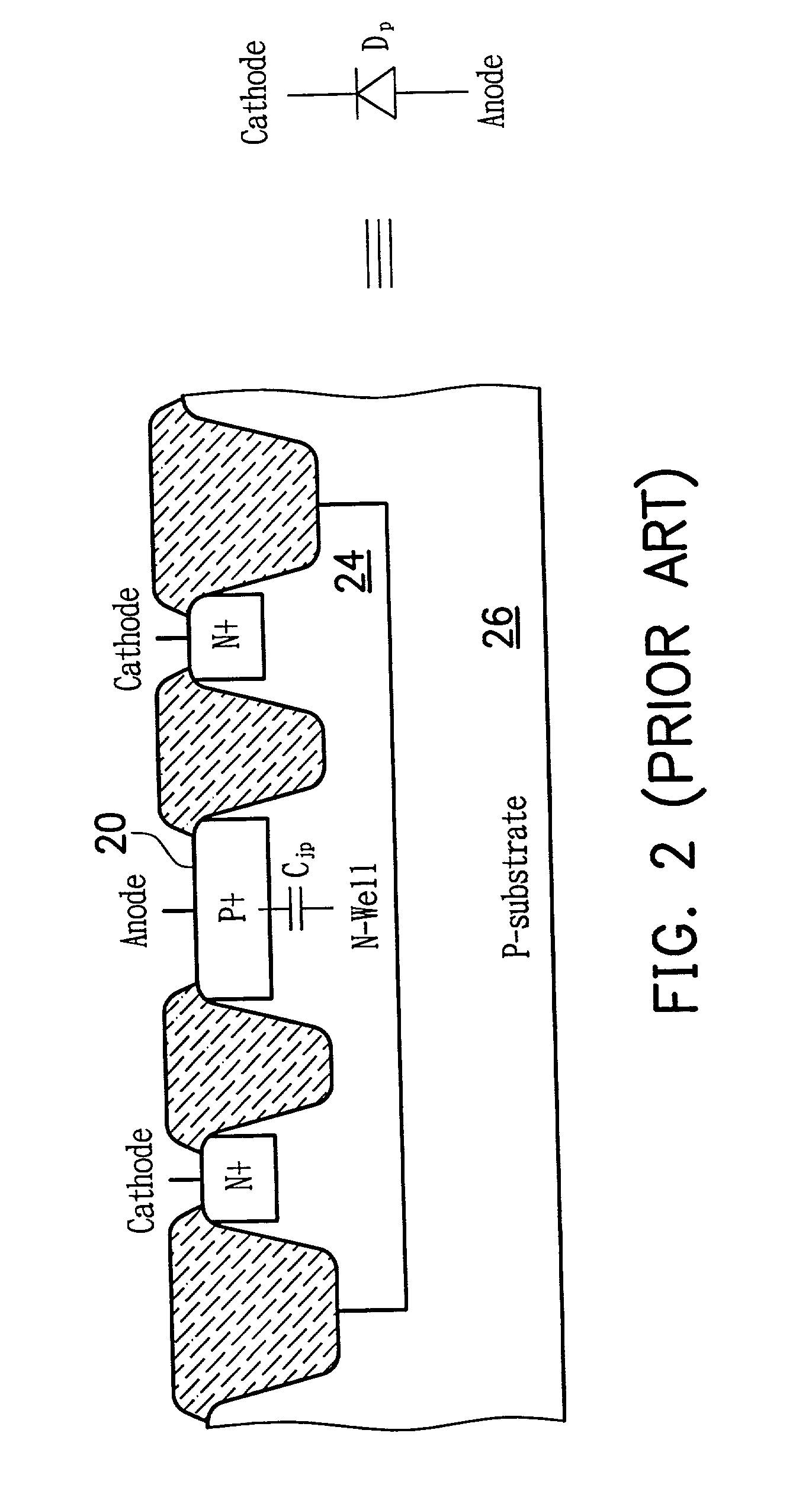
[0039] In order to reduce the input equivalent capacitance, the present invention proposes a stack structure of diodes as ESD protection circuit, as shown in FIG. 6. Two n-type diodes (D.sub.n1 and D.sub.n2) stack between a pad 30 and a power line VSSA. Two p-type diodes (D.sub.p1 and D.sub.p2) stack between the pad 30 and VDDA. During the normal operation of an integrated circuit, D.sub.p1, D.sub.p2, D.sub.n1, D.sub.n2 are reverse-biased but not breakdown, such that electrical signals at the pad 30 can be transmitted to the internal circuit 32. The values of the parasitic capacitance of the diodes are represented by C.sub.jn1, C.sub.jn2, C.sub.jp1 and C.sub.jp2, as shown in FIG. 6. Because of the stack structure, the equivalent capacitance input can be effectively reduced. For example, set C.sub.jn1=C.sub.jn2=C.sub.jn and C.sub.jp1=C.sub.jp2=C.sub.jp, the input equivalent capacitance C.sub.input becomes

C.sub.input=C.sub.pad+(C.sub.jn+C.sub.jp) / 2

[0040] In comparison to the conventio...


PUM


Abstract

The present invention proposes an ESD protection circuit with low input capacitance, suitable for an I/O pad. The ESD protection circuit includes a plurality of diodes and a power-rail ESD clamp circuit between power lines. The diodes are stacked and coupled between a first power line and the I/O pad. The ESD protection circuit between power lines is coupled between the first power line and a second power line. During normal operation, the diodes are reverse-biased and the ESD protection circuit between power lines is turned off. When an ESD event between the power line and the I/O pad occurs, the diodes are forward-biased, and the ESD protection circuit between power lines is turned on to conduct ESD current. The equivalent input capacitance of the ESD protection circuit of the present invention is very small, making it particularly suitable for the I/O port of high-frequency or high-speed IC.

Description

BACKGROUND OF THE INVENTION[0001] 1. Field of the Invention[0002] The present invention relates to an electrostatic discharge (ESD) protection circuit with low capacitance, in particular, to an ESD protection circuit suitable for high-frequency I / O ports.[0003] 2. Description of the Related Art[0004] As the manufacturing process for integrated circuit (IC) improves, the gate oxide layer of metal-oxide-semiconductor transistors (MOS) becomes thinner and more easily damaged by unexpected stress. Thus, it has become more and more important to provide effective ESD protection circuit in I / O ports or between power supply lines to prevent internal elements from being damaged by ESD stress.[0005] FIG. 1(a) is a conventional ESD protection circuit composed of two diodes, being put between an input / output (I / O) pad 10 and an internal circuit 12. P-type diode D.sub.p1 is connected between VDD and I / O pad 10, n-type diode D.sub.n1 is connected between VSS and I / O pad 10. FIG. 1(b) is an improv...

Claims


Application Information

Patent Timeline
IPC IPC(8): H01L27/02H01L29/861
CPCH01L27/0255H01L27/0292H01L29/8611
Inventor KER, MING-DOUCHANG, HUN-HSIENWANG, WEN-TAI
Owner TAIWAN SEMICON MFG CO LTD
Why Eureka
Try Eureka