Sloped trench etching process

a trench etching and slope technology, applied in the direction of acceleration measurement using interia forces, instruments, coatings, etc., can solve the problems of high undesirable difficulty in suitably addressing, and difficulty in trench profiles where the substrate is undercut with respect to a patterning mask or the appearance of cusping under the mask is high

Inactive Publication Date: 2002-11-14
INST OF MICROELECTRONICS A SINGAPORE COMPANY LIMITED BY GUARANTEE
View PDF2 Cites 134 Cited by
  • Summary
  • Abstract
  • Description
  • Claims
  • Application Information

AI Technical Summary

Problems solved by technology

The fabrication of such trenches, however, presents a number of difficulties which are not suitably addressed by many existing processes.
For example, trench profiles where the substrate is undercut with respect to a patterning mask or where "cusping" is exhibited under the mask is highly undesirable.
In applications where a tapered trench profile is desired for better metal interconnect step-coverage, the slope of the trench becomes even more critical.
Also, very deep trenches cannot be etched utilizing these processes without overheating the resist.
This causes further resist flow which, in turn, results in a loss of etch profile control
Existing deep trench etching processes, however, provide sidewalls which are vertical or very nearly vertical, and this makes it difficult to carry out subsequent etch processing as the steep wall profile gives rise to stingers.
Lack of Suitable and Controllable Etch Chemistry
As the resist and silicon are etched at the same time, it is difficult to control one

Method used


Image

  • Sloped trench etching process
  • Sloped trench etching process
  • Sloped trench etching process

Examples


Embodiment Construction

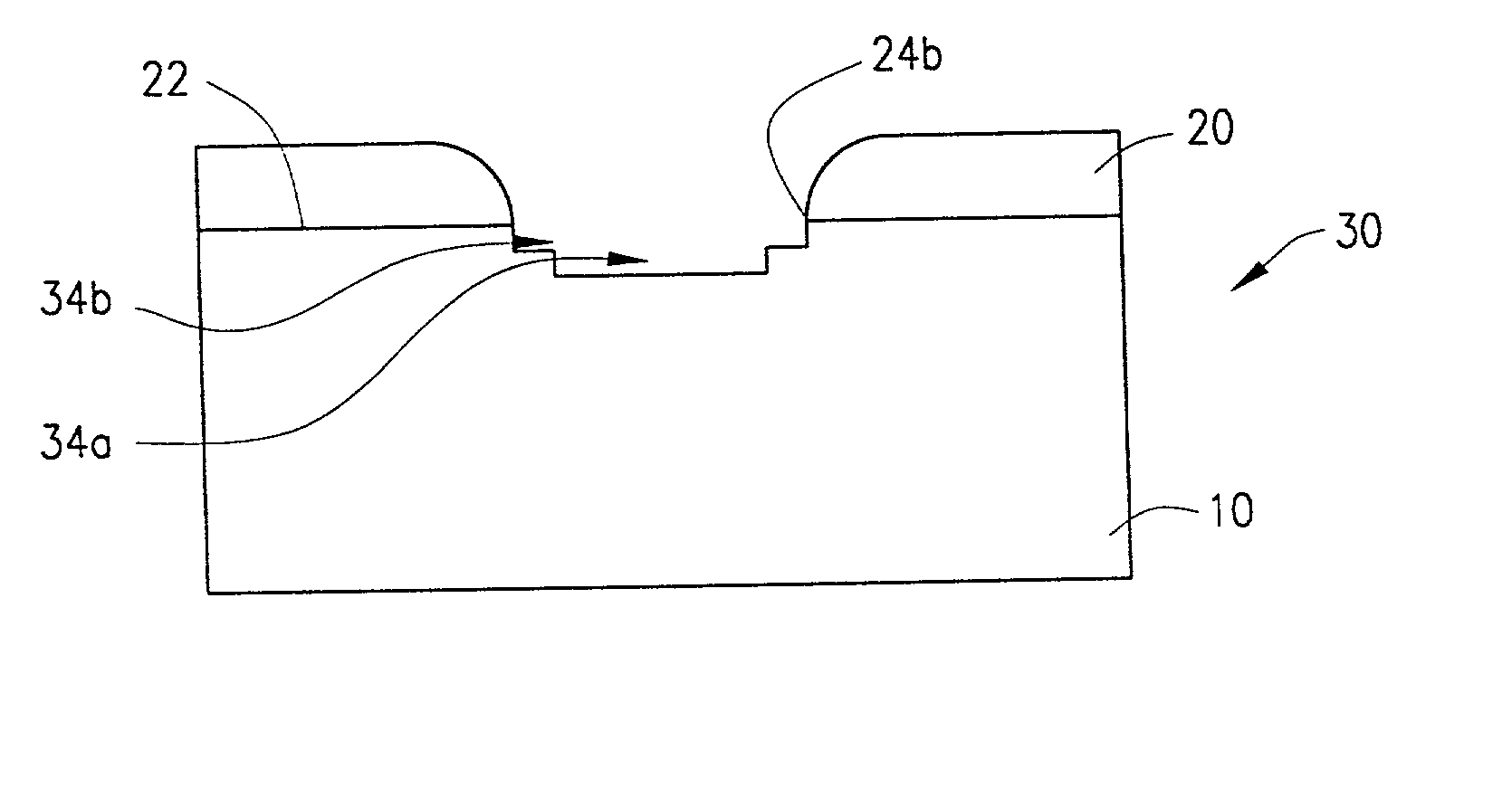
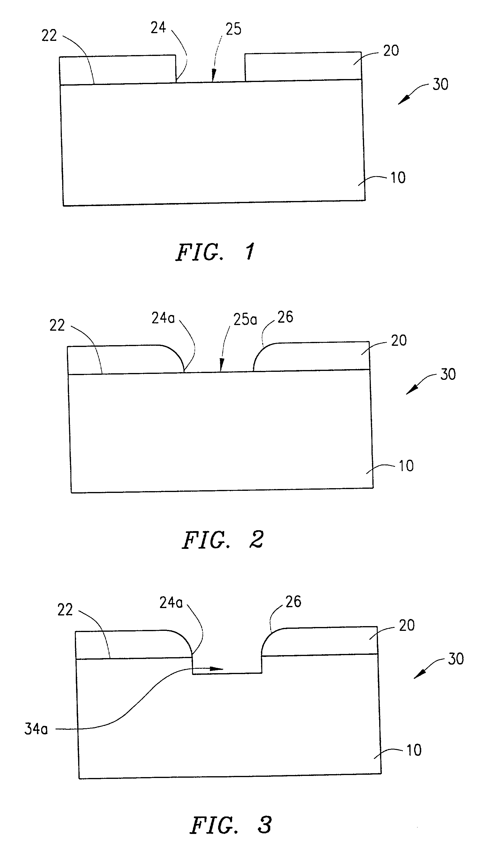
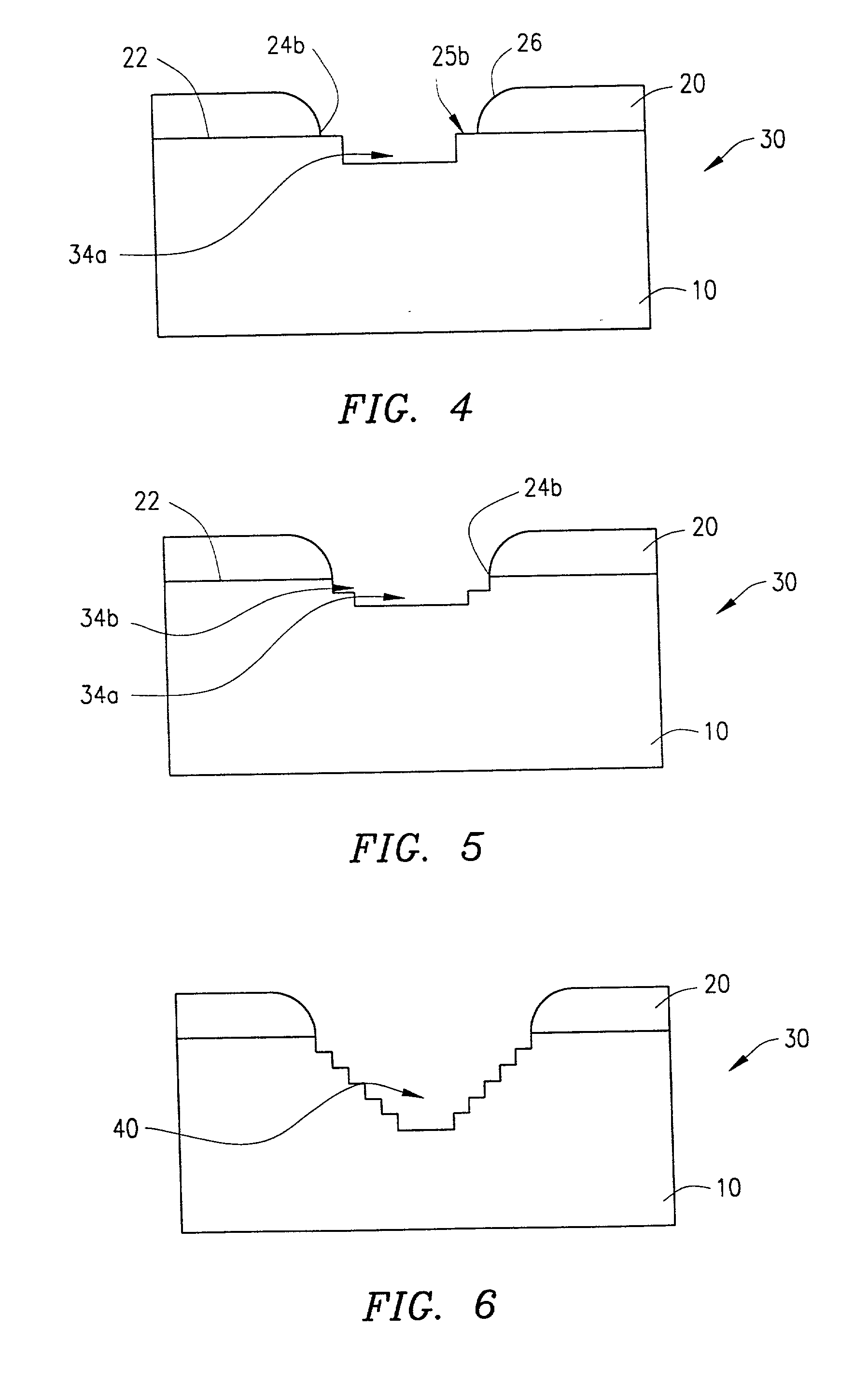
[0032] FIGS. 1-7 schematically illustrate steps of a sloped trench etching process according to a presently preferred embodiment of the invention, and FIG. 8 is a flow chart which summarizes steps of the process.

[0033] FIG. 1 illustrates a semiconductor substrate, for example, a silicon substrate, in which a trench is to be formed. The substrate is generally designated by reference number 10; and, as shown in FIG. 1, is initially provided with a mask member in the form of a resist layer 20 on upper surface 22 thereof from which the trench is to extend into the substrate. The substrate 10 having the resist layer 20 thereon is sometimes generally referred to herein as a wafer 30. As also shown in FIG. 1, the resist layer 20 includes a suitably formed and located opening 24 therein which defines an exposed area or region 25 on the surface 22 of the substrate 10 at which the trench is to be formed.

[0034] Although it is not essential to the practice of the method of the present invention...


PUM

PropertyMeasurementUnit
Lengthaaaaaaaaaa
Angleaaaaaaaaaa
Angleaaaaaaaaaa

Abstract

Method and apparatus for etching a tapered trench in a layer of material with a highly controllable wall profile. The layer of material has a mask adjacent a surface thereof having an opening which defines a location on the layer of material at which the trench is to be formed. Vertical etch process steps and opening enlarging process steps are then performed in an alternating manner until the trench has been etched to a desired depth. The method permits very deep tapered trenches of up to 80-100 um or more to be formed in a silicon substrate or other layer of material in a highly controllable manner. The method can be incorporated into processes for manufacturing numerous devices including MEMS devices and high power RF devices such as LDMOS and VDMOS devices.

Description

[0001] 1. Field of the Invention[0002] The present invention relates generally to etching processes; and, more particularly, to a method and apparatus for etching tapered trenches in a layer of material with a controlled wall profile.[0003] 2. Description of the Prior Art[0004] The etching of trenches in a semiconductor substrate is an important part of the overall process of manufacturing many integrated circuit devices. The fabrication of such trenches, however, presents a number of difficulties which are not suitably addressed by many existing processes. For example, some of the more important problems that are associated with current trench etching processes include the following:[0005] Inadequate Trench Sidewall Profile Control[0006] The trench sidewall profile is of particular concern in many applications. For example, trench profiles where the substrate is undercut with respect to a patterning mask or where "cusping" is exhibited under the mask is highly undesirable. Even min...

Claims


Application Information

Patent Timeline
IPC IPC(8): B81C1/00G01P15/08H01L21/308
CPCG01P15/0802H01L21/3086B81B2203/0384B81B2203/033B81C1/00103
Inventor NAGARAJAN, RANGANATHAN
Owner INST OF MICROELECTRONICS A SINGAPORE COMPANY LIMITED BY GUARANTEE
Why Eureka
Try Eureka