Point emission type light emitting element and concentrating point emission type light emitting element

a technology of light emitting elements and light emitting elements, which is applied in the direction of lasers, semiconductor devices, semiconductor lasers, etc., can solve the problems that the light emitting element that restricts the light emitting area within the microscopic region cannot be provided at an economical price, and are unsuitable for such applications

Inactive Publication Date: 2002-11-14
NICHIA CORP
View PDF2 Cites 10 Cited by
  • Summary
  • Abstract
  • Description
  • Claims
  • Application Information

AI Technical Summary

Problems solved by technology

This results in the problem that the light emitting element that restricts the light emitting area within the microscopic region cannot be provided at an economical price.
Although the end face emission type light emitting diode can be made with small spot size, multi-mode light emission is produced sin

Method used


Image

  • Point emission type light emitting element and concentrating point emission type light emitting element
  • Point emission type light emitting element and concentrating point emission type light emitting element
  • Point emission type light emitting element and concentrating point emission type light emitting element

Examples


first embodiment

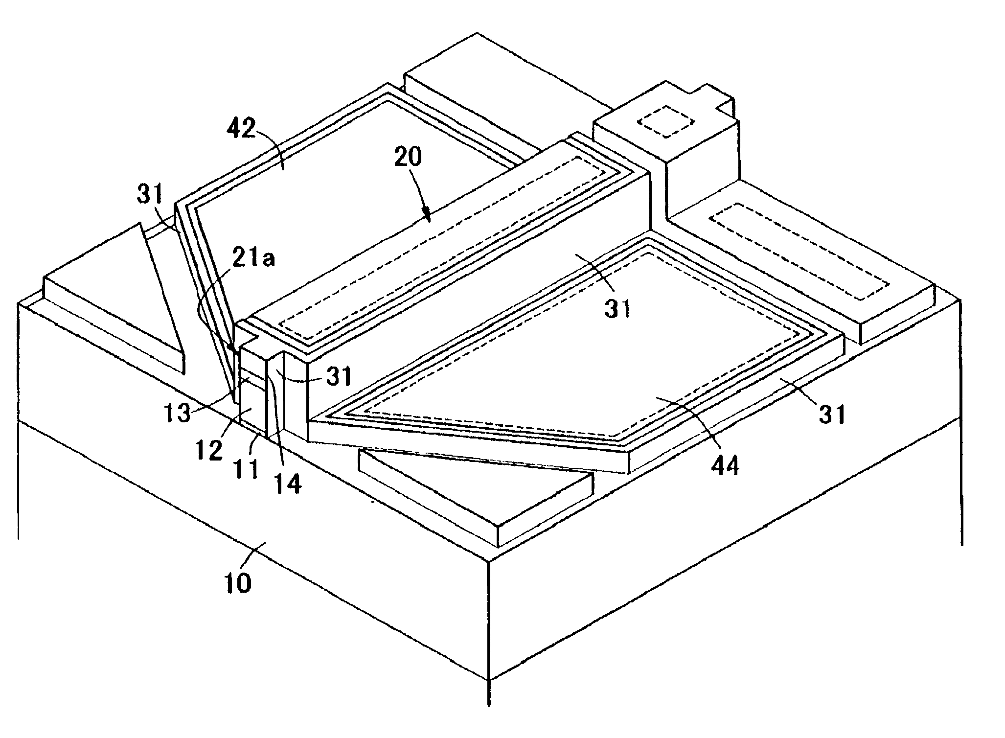
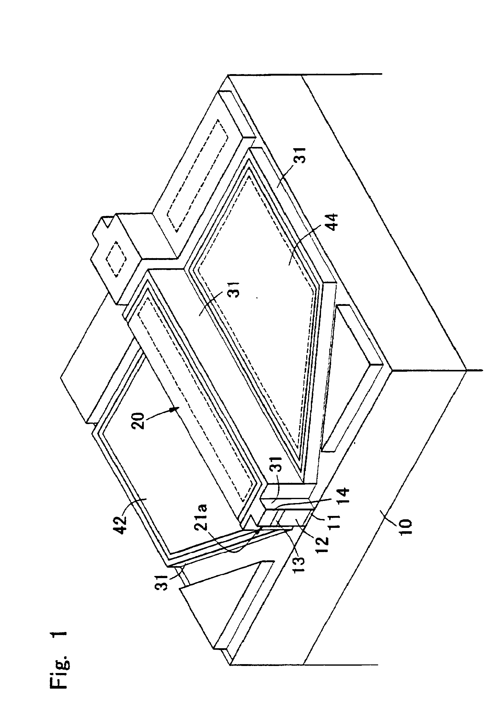
[0048] The point emission type light emitting element according to the present invention is a nitride semiconductor light emitting diode. The point emission type light emitting element has such a constitutions as an n-type layer 12, an active layer 13 and a p-type layer 14 that are formed from nitride semiconductors on a substrate 10 made of sapphire via a buffer layer 11, with a stripe ridge 20 that has a protruding portion 21a being formed on one end face thereof, while being covered with an shading film 31 substantially entirely except for the tip of the protruding portion 21a, as shown in FIG. 1. The point emission type light emitting element is manufactured as described below.

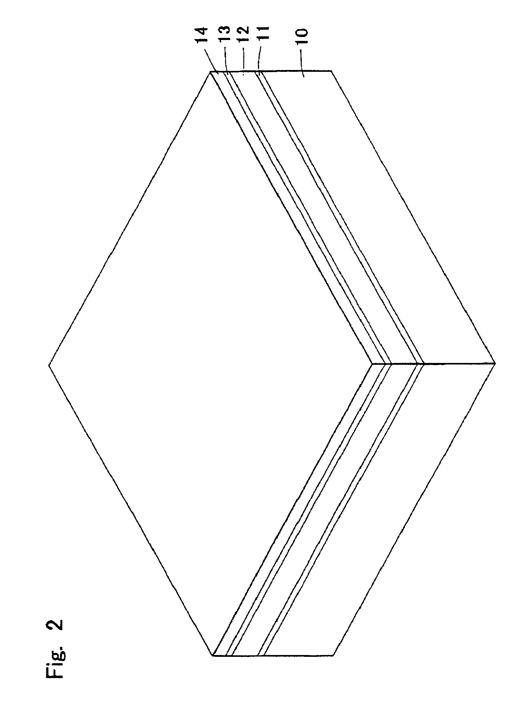
[0049] First, as shown in FIG. 2, the buffer layer 11 made of GaN grown at a low temperature, for example, the n-type layer 12 made of GaN doped with Si, for example, the active layer 13 made of InGaN, for example, and the p-type layer 14 made of GaN doped with Mg, for example, are formed successively on t...

embodiment 1

VARIATION OF EMBODIMENT 1

[0076] For the substrate used in the present invention, insulating substrate such as sapphire or spinel (MgAl.sub.2O.sub.4) that has principal plane in C plane, R plane or A plane, SiC (including 6H, 4H, 3C), ZnS, ZnO, GaAs, Si and oxide substrate that makes lattice matching with nitride semiconductor have been known as materials different from nitride semiconductor. Sapphire and spinel are preferably used. A nitride semiconductor substrate such as GaN and AlN can also be used.

[0077] As the nitride semiconductor formed on the substrate, III-V group gallium nitride compound semiconductor materials can be used. For example, In.sub.xAl.sub.yGa.sub.1-x-yN (0.ltoreq.x.ltoreq.1, 0.ltoreq.y.ltoreq.1, 0.ltoreq.x+y.ltoreq.1), and InAlGaBN, InAlGaNP and InAlGaNAs made by adding B to the III group element or substituting a part of V group element N with As or P can be used. Good light emitting layer can be obtained by using In.sub.uAl.sub.vGa.sub.1-u-vN (0

embodiment 2

VARIATION OF EMBODIMENT 2

[0125] Although the reflector surface having conical shape is constituted from the cavity 152 of conical shape in the second embodiment, the present invention is not limited to this constitution and a refracting surface having conical shape may be formed as described below, so that concentrated light is output from the light emitting point.

[0126] Specifically, as shown in FIG. 18, in the stacked semiconductor structure located right below the light emitting point, such a recess of pyramidal shape is formed so as to reach at least the n-type semiconductor layer that expands toward the light emerging point, and the recess is filled with a transparent material 152a that has a refractive index higher than that of the active layer.

[0127] With the constitution described above, light emitted in the light emitting regions and directed toward the light emerging point is refracted due to the difference in the refraction index between the semiconductor layer (mainly th...


PUM


Abstract

To provide a point emission type light emitting element that restricts the light emitting area within a sufficiently tiny region and can be manufactured at a low cost, the point emission type light emitting element is a light emitting element that has stripe ridge comprising an n-type layer, an active layer and a p-type layer that are formed from semiconductors on a substrate, so as to emit light from one end face of the stripe ridge, wherein the stripe ridge has a protruding portion on the end face described above and the surface of the light emitting element is covered with an shading film except for the tip of the protruding portion.

Description

[0001] b 1. Field of the Invention[0002] The present invention relates to a point emission type light emitting element having a light emitting area restricted within a tiny region, and to a concentrating point emission type light emitting element that concentrates light emitted thereby and outputs the light through a tiny region.[0003] 2. Description of the Related Art[0004] The present applicant already developed nitride semiconductor light emitting diodes that emit blue and green light with high output power and are used in practical applications as light sources for large image display apparatuses. The nitride semiconductor light emitting element is manufactured, for example, by forming p-type and n-type ohmic electrodes on a multi-layer semiconductor film that is formed from a nitride semiconductor of GaN, AlN, InN or a mixed crystal thereof on a sapphire substrate, and separating the elements into chips by such processes as cleaving, RIE etching or dicing. The light emitting el...

Claims


Application Information

Patent Timeline
IPC IPC(8): H01L33/10H01L33/20H01L33/32H01S5/00H01S5/028H01S5/042H01S5/185H01S5/22H01S5/227
CPCH01S5/005H01S5/0286H01S5/0425H01S2301/18H01S5/22H01S5/2275H01S5/1082H01S5/04254H01S5/04256H01S5/04257H01S5/04252H01S5/4056H01S5/02255H01S5/185
Inventor MARUTANI, YUKITOSHIKITANO, AKIRAHARADA, SUSUMUAKAISHI, KAZUYUKISANO, MASAHIKOHONJO, KOJIMAEGAWA, HITOSHI
Owner NICHIA CORP
Why Eureka
Try Eureka