Integration of High K Gate Dielectric

Inactive Publication Date: 2002-11-21
ASM IP HLDG BV
View PDF20 Cites 142 Cited by
  • Summary
  • Abstract
  • Description
  • Claims
  • Application Information

AI Technical Summary

Benefits of technology

0019] The present invention provides methods for improving deposition over high k materials, with k values over 7, such as aluminum oxide (Al.sub.2O.sub.3), zirconium oxide (ZrO.sub.2), hafnium oxide (HfO.sub.2), tantalum oxide (Ta.sub.2O.sub.5), barium strontium titanate (BST), strontium bismuth tantalate (SBT), and various lanthanide (rare earth) oxides. The invention is illustrated in the context of transistor gate stacks, where silicon-based materials are deposited over high k gate dielectrics.
0020] The inventors have found that traditional methods of depositing silicon-containing materials, such as polysilicon and poly-SiGe, over high k dielectrics tend to results in poor electrical performance of resultant devices. One possible reason for this poor performance identified by the inventors is the reduction of oxides Accordingly, processes are provided herein for depositing electrode materials, preferably silicon-containing layers, over high k materials while minimizing reduction of the high k materials. At least during an initial seed phase, deposition conditions are arranged to minimize diffusion of hydrogen to the high k material. Preferably, a second or bulk phase of deposition includes altered conditions arranged to increase the deposition rate such that overall throughput for the deposition is not excessively affected. However, conditions during even the bulk phase are preferably arranged to reduce hydrogen diffusion to the high k material, relative to con

Problems solved by technology

The inventors have found that traditional methods of depositing silicon-containing materials, such as polysili

Method used


Image

  • Integration of High K Gate Dielectric
  • Integration of High K Gate Dielectric
  • Integration of High K Gate Dielectric

Examples


Embodiment Construction

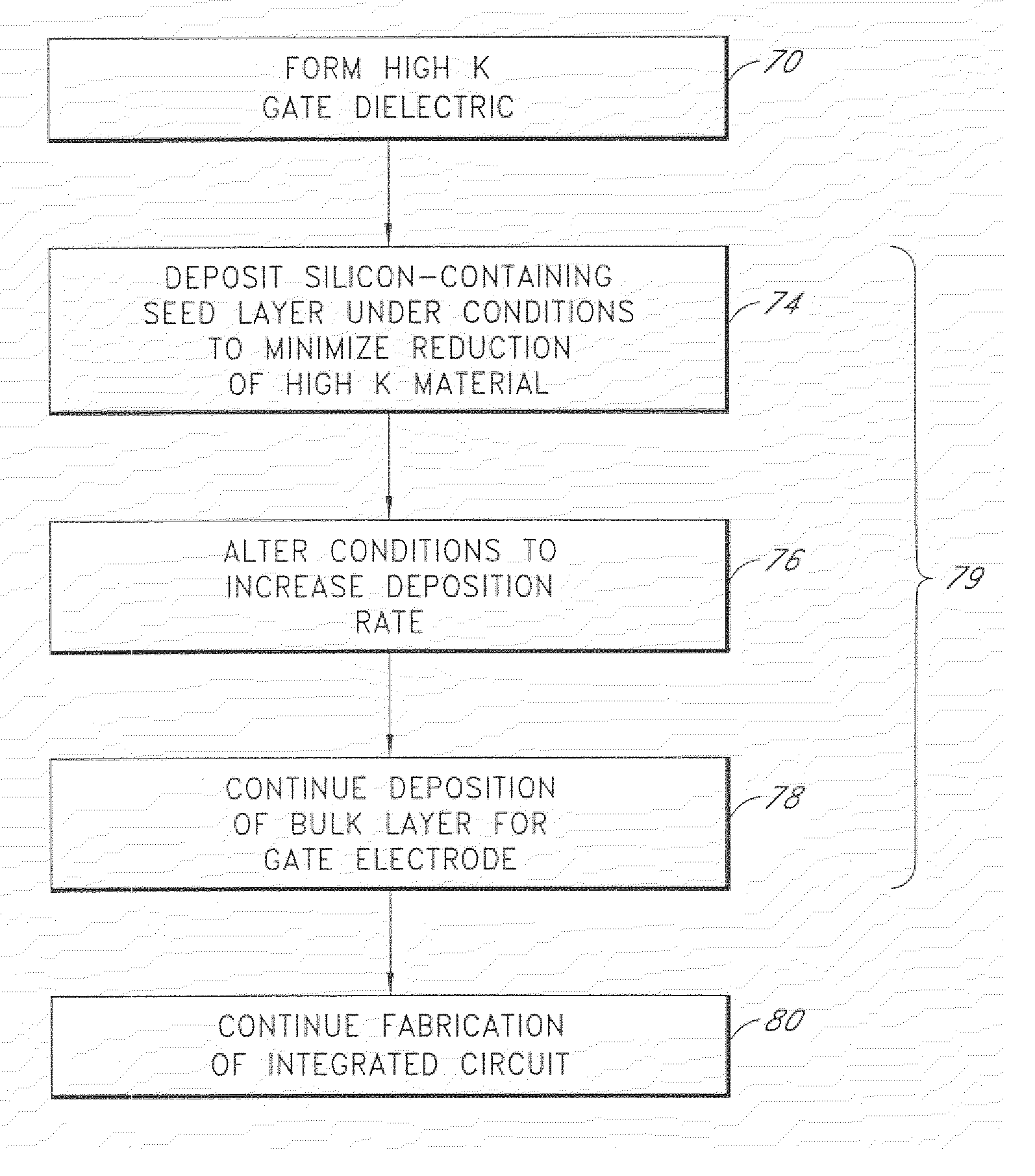
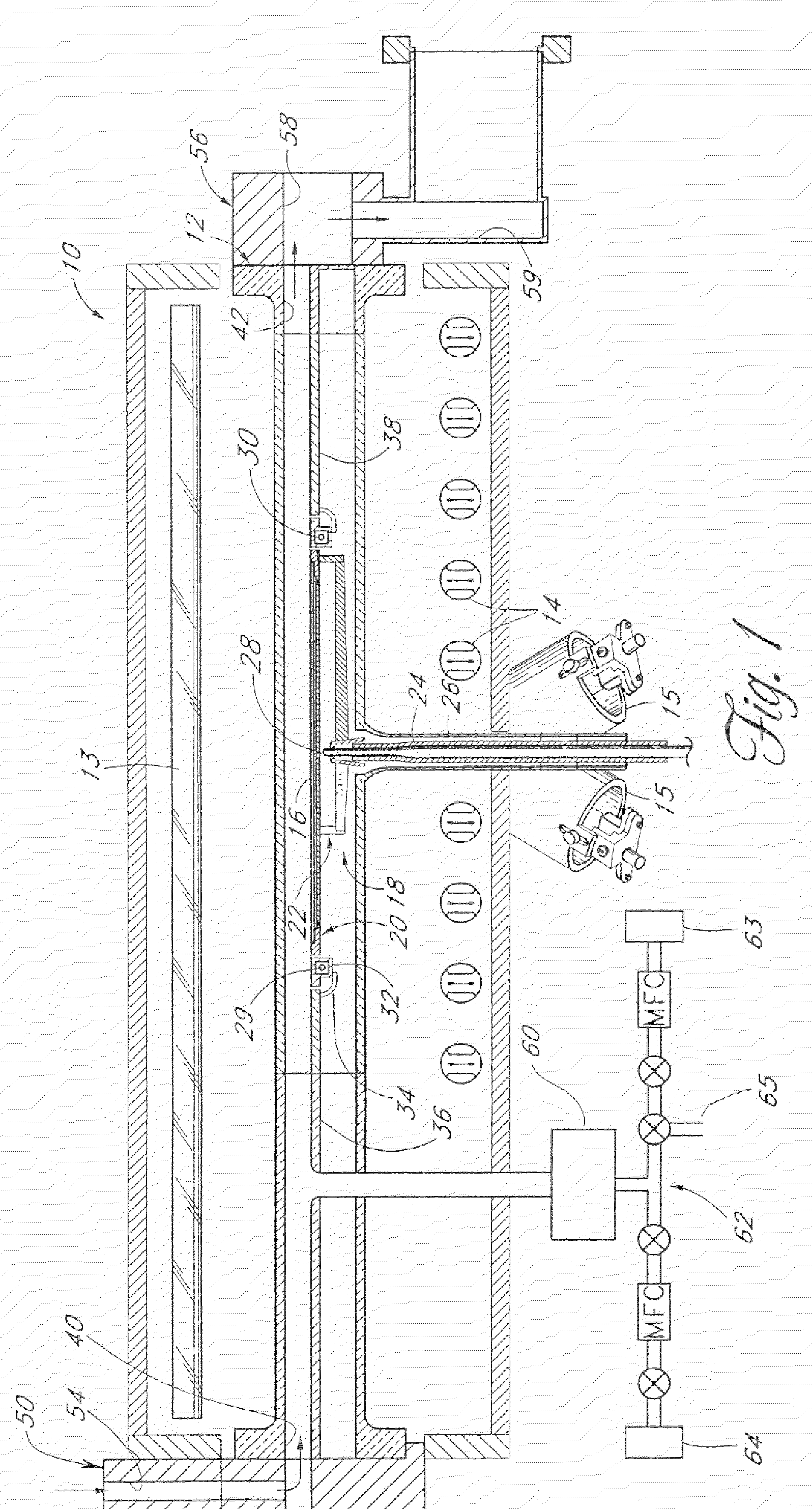
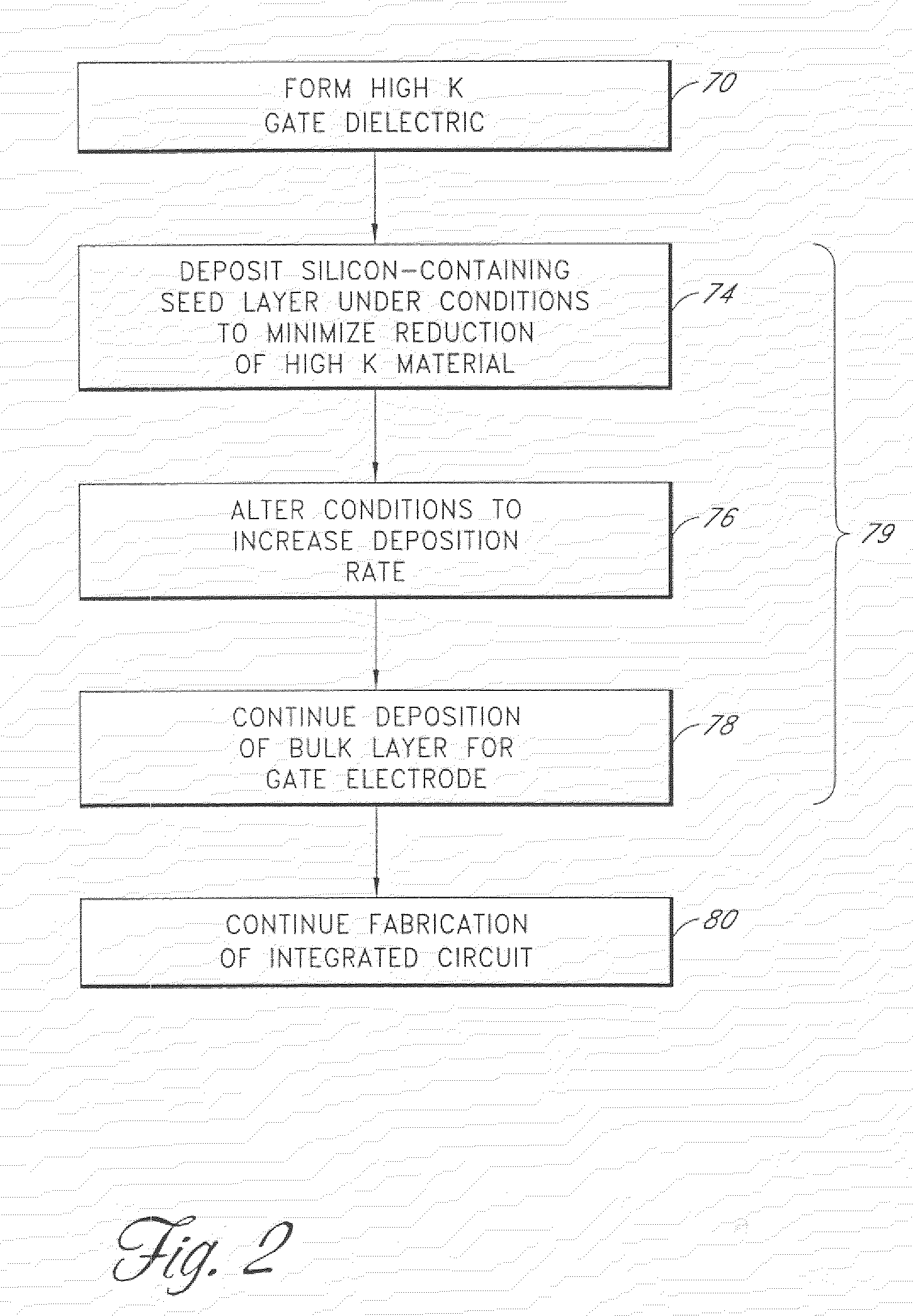
[0025] While the preferred embodiments are described in the context of transistor gate stacks, the skilled artisan will readily appreciate that the principles disclosed herein have application to a variety of contexts in which layers must be deposited over high k materials. An example of such a context is in the formation of capacitor electrodes over high k dielectrics, proposed for high density memory cells in random access memory (RAM) arrays. The methods described herein are particularly advantageous for depositing silicon-containing layers over high k materials, but the skilled artisan will also appreciate applications of the principles and advantages described herein to depositing metallic electrodes over high k materials.

[0026] As noted in the Summary section above, conventional gate electrode deposition over high k gate dielectrics has been found to result in poor electrical performance of the resultant devices. In order to increase the reliability and yield of the integrated...


PUM

PropertyMeasurementUnit
Partial pressureaaaaaaaaaa
Pressureaaaaaaaaaa

Abstract

<heading lvl="0">Abstract of Disclosure</heading> Methods are provided herein for forming electrode layers over high dielectric constant (high k) materials. In the illustrated embodiments, a high k gate dielectric, such as zirconium oxide, is protected from reduction during a subsequent deposition of silicon-containing gate electrode. In particular, a seed deposition phase includes conditions designed for minimizing hydrogen reduction of the gate dielectric, including low hydrogen content, low temperatures and/or low partial pressures of the silicon source gas. Conditions are preferably changed for higher deposition rates and deposition continues in a bulk phase. Desirably, though, hydrogen diffusion is still minimized by controlling the above-noted parameters. In one embodiment, high k dielectric reduction is minimized through omission of a hydrogen carrier gas. In another embodiment, higher order silanes aid in reducing hydrogen content for a given deposition rate.

Description

Cross Reference to Related Applications[0001] This application claims the priority benefit under 35 U.S.C. .sctn.119(e) to provisional application No. 60 / 268,337, filed February 12, 2001; provisional application No. 60 / 279,256, filed March 27, 2001; and provisional application No. 60 / 332,696, filed November 13, 2001.Background of InventionField of the Invention[0002] The invention relates generally to forming semiconductor layers in integrated circuit fabrication, and more particularly to forming gate electrodes over high dielectric constant (high k) gate dielectrics in a transistor gate stack.Background of the Invention[0003] Integrated circuit design is constantly being scaled down in pursuit of faster circuit operation and lower power consumption. Scaled dimensions in a circuit design generally requires attendant changes in fabrication processing.[0004] A basic building block of integrated circuits is the thin film transistor (TFT). As is known in the art, the transistor typicall...

Claims


Application Information

Patent Timeline
IPC IPC(8): C23C16/02C30B25/02H01L21/20H01L21/205C23C16/24H01L21/28H01L21/285H01L21/3205H01L21/336H01L21/4763H01L21/8242H01L27/108H01L29/423H01L29/49H01L29/51H01L29/78H01L29/786H01L31/18H01L31/20
CPCB82Y10/00H01L21/02502C30B25/02C30B29/06H01L21/28035H01L21/28044H01L21/28194H01L21/28525H01L21/28556H01L29/4925H01L29/517H01L31/1804H01L31/182H01L31/202Y02E10/546Y02E10/547H01L21/02381H01L21/02532H01L21/0262H01L21/02661H01L21/0245H01L21/02488C23C16/0272Y02P70/50
Inventor POMEREDE , CHRISTOPHE F.GIVENS , MICHAEL E.SHERO , ERIC J.TODD , MICHAEL A.
Owner ASM IP HLDG BV
Why Eureka
Try Eureka