
Method to grow self-assembled epitaxial nanowires

a technology of epitaxial nanowires and nanowires, which is applied in the field of self-assembling nanowires, can solve the problems of difficult to achieve, irregular shape and size, and wire-like structure, and achieve the effects of reducing manufacturing costs, simplifying manufacturing processes, and high crystal quality

Inactive Publication Date: 2003-01-09
HEWLETT PACKARD DEV CO LP
View PDF0 Cites 38 Cited by
  • Summary
  • Abstract
  • Description
  • Claims
  • Application Information

AI Technical Summary

Benefits of technology

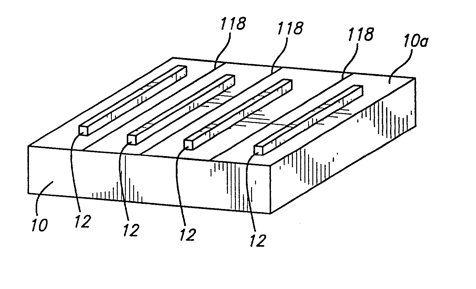
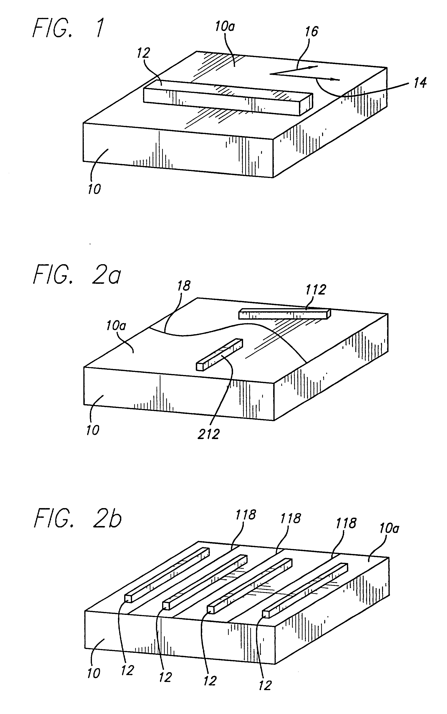
[0009] The present invention provides a means to grow one-dimensional epitaxial crystals with widths and heights at the nanometer scale, and lengths at the micrometer scale, which are aligned along certain crystallographic directions with high crystal quality. Further, the present invention avoids traditional lithography-deposition-etching methods, minimizes defects formed during the normal lithography process and environmental toxic chemicals usage, simplifies the manufacturing processes, and allows self-assembled formation of high-quality one-dimensional nano-wires over large areas.

Problems solved by technology

However, the formation of robust "one"-dimensional nanowires with a width less than 10 nm has been a major goal that has proven difficult to achieve by either epitaxial growth or lithographic processing.
However, they often produce wire-like structures that meander along with the steps, are terminated by single steps, have irregular shapes and sizes, and / or are not robust.
These lattice-mismatched systems will thus limit the lateral growth in all directions on the substrate surface and produce strained islands.
However, because of the large lattice mismatches along both directions, the sizes and shapes of the PtSi islands were quite heterogeneous.

Method used


Image

  • Method to grow self-assembled epitaxial nanowires
  • Method to grow self-assembled epitaxial nanowires
  • Method to grow self-assembled epitaxial nanowires

Examples


example 1

ErSi.sub.2

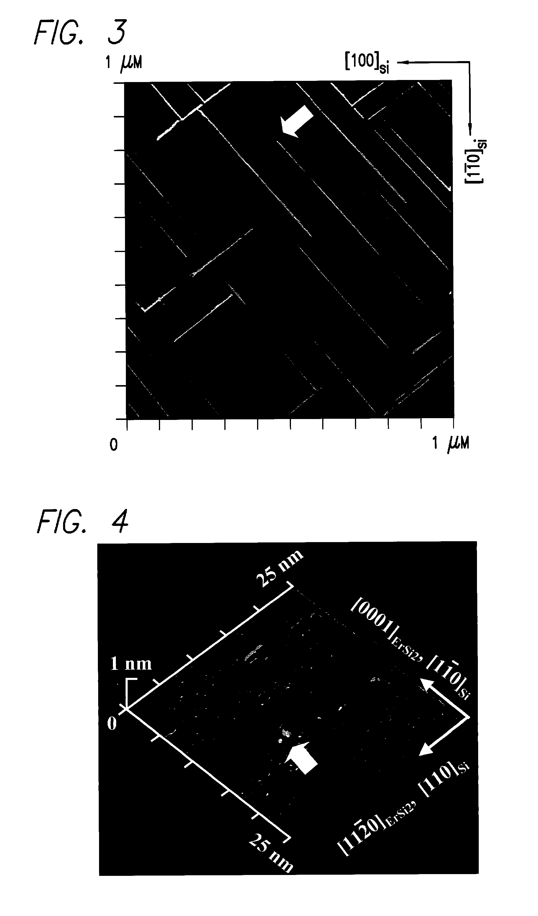
[0036] The following example demonstrates that by utilizing an epitaxial overlayer that has a carefully chosen lattice mismatch to complement the host substrate, in this case erbium disilicide (ErSi.sub.2) on Si(001), it is possible to grow nanowires. Due to its high conductivity (2.9.times.10.sup.4 (.OMEGA.cm).sup.-1) and low Schottky barrier to n-type Si, ErSi.sub.2 thin films grown on Si substrates have been studied extensively. These studies involved continuous thin films on Si(001) that were several nanometers thick, and they revealed oriented crystallites with a hexagonal A1B.sub.2-type crystal structure that were thermodynamically stable in contact with Si below 800.degree. C. The axis of the ErSi.sub.2 was oriented along a -10> axis of the Si(001) substrate, and the [11{overscore (2)}0] of the ErSi.sub.2 was oriented along the perpendicular .cent.110> axis, with lattice mismatches of +6.5% and -1.3%, respectively, which nearly satisfies the proposed growth conditio...

examples 2-5

ErSi.sub.2, SCSi.sub.2, DySi.sub.2, GdSi.sub.2 and Their Comparison

[0045] In the following experiments, device quality "flat" Si(001) substrates were prepared as in Example 1.

[0046] As measured from STM images, the average terrace widths along [110].sub.Si and [1{overscore (1)}0].sub.Si were 57.8 nm and 21.3 nm, respectively, implying that the normal direction of the surface of the Si substrate used in these experiments was misoriented from [001].sub.Si toward [120].sub.Si by about 0.4.degree..

[0047] The final state of the nanowires was influenced by their growth conditions, such as deposition and annealing temperature, deposition rate, coverage of deposited atoms, and annealing time. The physical properties of Sc, Er, Dy, and Gd are similar (e.g., their melting points are 1539.degree. C., 1522.degree. C., 1409.degree. C., and 1314.degree. C. respectively), and the experimentally-determined growth conditions for producing dislocation-free nanowires are also very close. The optimum s...


PUM

PropertyMeasurementUnit
lengthaaaaaaaaaa
lengthaaaaaaaaaa
heightaaaaaaaaaa

Abstract

Self-assembled nanowires are provided, comprising nanowires of a first crystalline composition formed on a substrate of a second crystalline composition. The two crystalline materials are characterized by an asymmetric lattice mismatch, in which in the interfacial plane between the two materials, the first material has a close lattice match (in any direction) with the second material and has a large lattice mismatch in all other major crystallographic directions with the second material. This allows the unrestricted growth of the epitaxial crystal in the first direction, but limits the width in the other. The nanowires are grown by first selecting the appropriate combination of materials that fulfill the foregoing criteria. The surface of the substrate on which the nanowires are to be formed must be cleaned in order (1) to ensure that the surface has an atomically flat, regular atomic structure on terraces and regular steps and (2) to remove impurities. Finally, epitaxial deposition of the first crystalline material on the cleaned surface is performed, thereby forming the self-assembled nanowires. Thus, one-dimensional epitaxial crystals are obtained with widths and heights at the nanometer scale, and lengths at the micrometer scale, which are aligned along certain crystallographic directions with high crystal quality.

Description

[0001] The present application is a non-provisional application and claims priority from provisional application Serial No. 60 / 300,440, filed on Jun. 26, 2001.[0002] The present invention is related generally to electronic devices whose functional scales are measured in nanometers, and, more particularly, to forming one-dimensional epitaxial crystals with widths and heights at the nanometer scale.[0003] The synthesis of artificial low-dimensional structures to confine electrons has been a topic of scientific and technical interest for decades. Epitaxial deposition techniques have made possible the growth of two-dimensional quantum wells as thin as one atomic layer and "zero"-dimensional islands as small as a few nanometers. However, the formation of robust "one"-dimensional nanowires with a width less than 10 nm has been a major goal that has proven difficult to achieve by either epitaxial growth or lithographic processing. Various "self-assembly" techniques, in which structures for...

Claims


Application Information

Patent Timeline
Patent Type & Authority Applications(United States)
IPC IPC(8): C30B23/02C30B25/02
CPCC30B23/02C30B25/02Y10T428/24802Y10T428/12674Y10T428/24942Y10T428/24917Y10S977/763C30B29/605Y10T428/249921
Inventor CHEN, YONGWILLIAMS, R. STANLEYOHLBERG, DOUGLAS A. A.
Owner HEWLETT PACKARD DEV CO LP
Learn More