Semiconductor device and manufacturing method

Inactive Publication Date: 2003-04-10
TEXAS INSTR INC
View PDF2 Cites 24 Cited by
  • Summary
  • Abstract
  • Description
  • Claims
  • Application Information

AI Technical Summary

Benefits of technology

[0003] In order to improve the reliability of the electrical connection (referred to as electrical reliability, hereinafter) in the semiconductor package, the solder balls and the conductor patterns must be joined more securely. Thus, it has been suggested that after the semiconductor package is attached to a motherboard (printed-wiring board), a resin called an underfill be supplied between the semiconductor package and the motherboard. However, supplying the underfill during post-processing not only complicates the production process but also makes supplying the underfill more difficult since the solder balls are more densely arranged.
[0004] In addition, a structure called a flip-chip, in which a semiconductor chip is mounted directly on the motherboard, has also been suggested in recent years. In the case of said flip-chip structure, solder bumps serving as external connection terminals are formed on electrode pads formed on the surface of the semiconductor chip. In the case of a semiconductor chip of said type, the solder bumps and the electrode pads must be joined more securely in order to improve the connection reliability. Thus, there is great demand for developing a technology for improving the connection reliability without complicating the production process.
[0005] Therefore, the purpose of the present invention is to present a semiconductor device and its manufacturing method with which the connection reliability can be improved but without complicating the production process.
[0009] As described above, when the conductive part containing the heat-curing epoxy resin is used, and heat treatment is applied in order for the heat-curing epoxy resin to form resin parts at the periphery of the external connection terminals during the formation of the external connection terminals, the external connection terminals can be reliably connected to the insulated substrate, so that the connection reliability in the semiconductor device can be improved. In addition, because the underfill supplying step during post-processing can be eliminated, the manufacturing process can be simplified.

Problems solved by technology

However, supplying the underfill during post-processing not only complicates the production process but also makes supplying the underfill more difficult since the solder balls are more densely arranged.

Method used


Image

  • Semiconductor device and manufacturing method
  • Semiconductor device and manufacturing method
  • Semiconductor device and manufacturing method

Examples


first embodiment

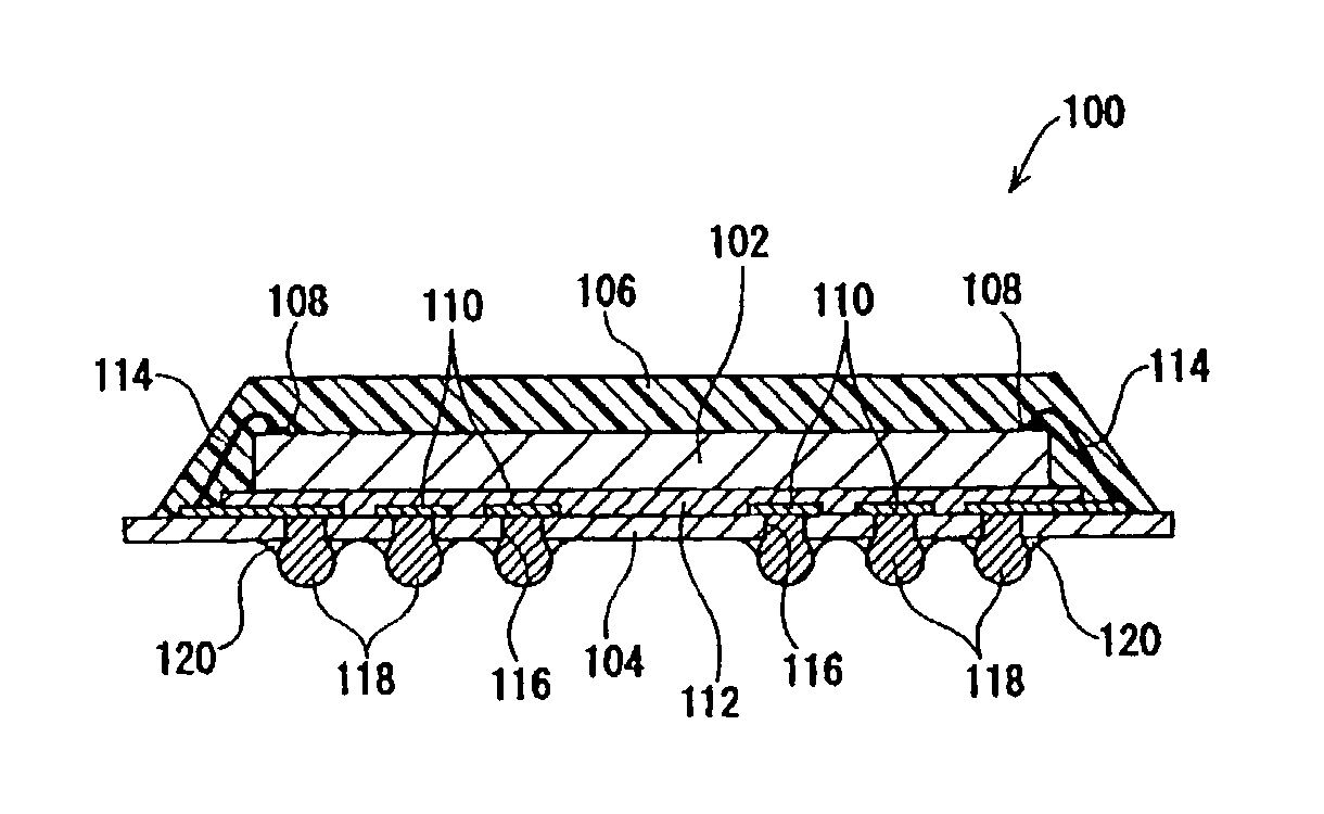
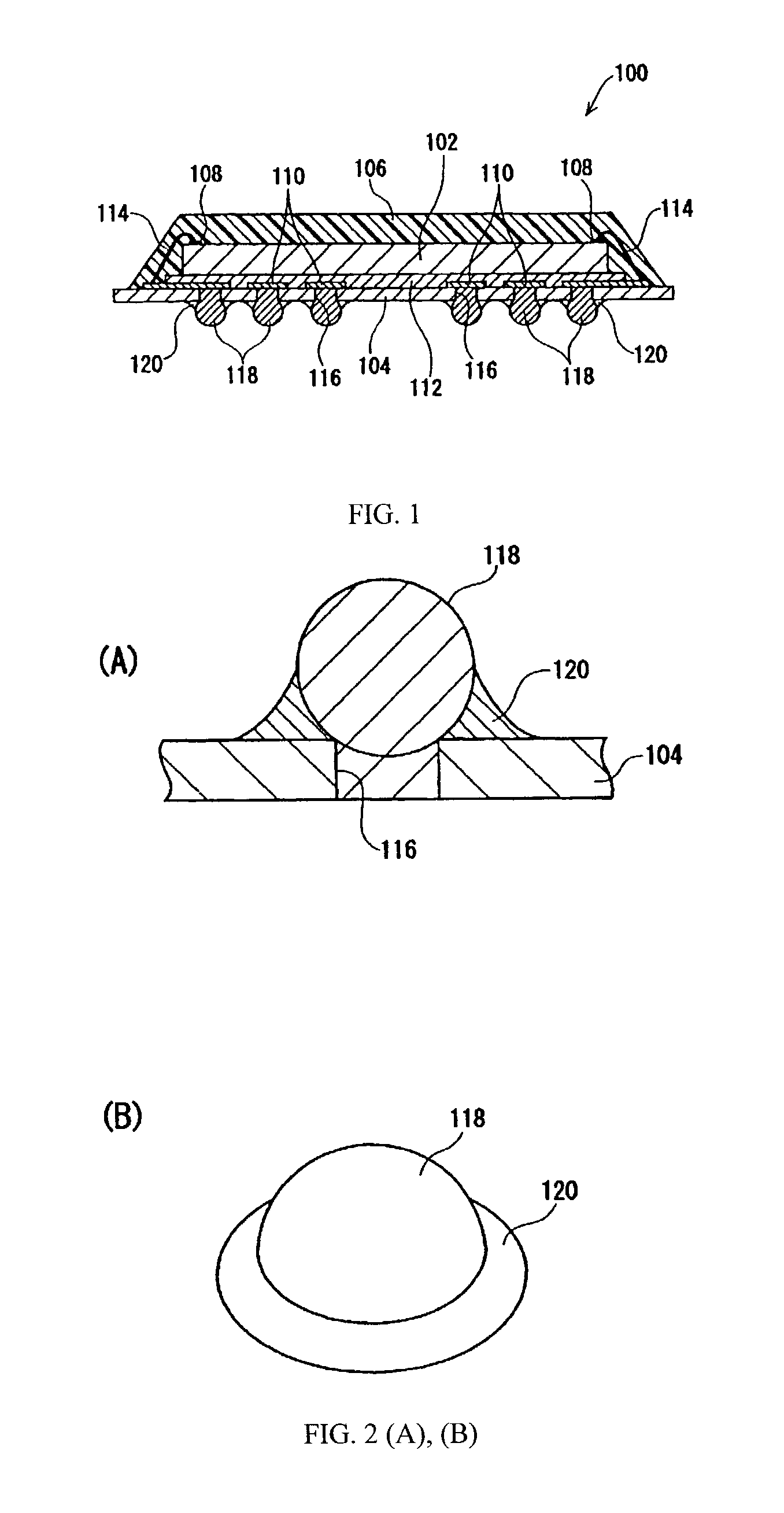
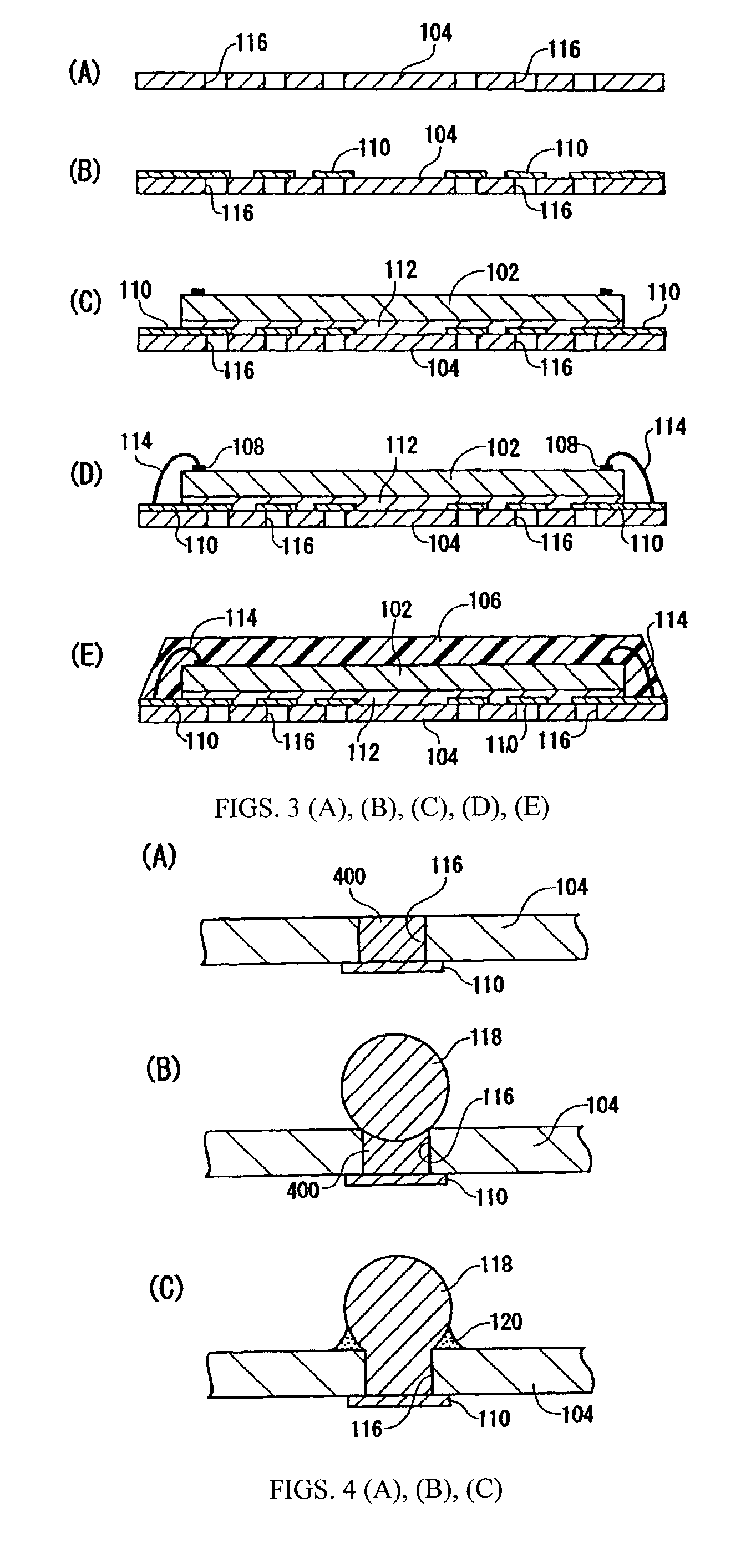
[0026] The present invention will be explained in detail below with reference to an embodiment illustrated by the figures. FIG. 1 is a cross section showing the structure of semiconductor package 100 pertaining to the present invention. Said semiconductor package 100 is called a BGA package provided with semiconductor chip 102 in which an integrated circuit is formed on the surface of an Si (silicon) substrate, insulated substrate 104 on which said semiconductor chip 102 is mounted, and sealing material 106 used to seal them. Electrode pads 108 led out from said integrated circuit are formed on the surface of semiconductor chip 102. Semiconductor chip 102 is bonded to the principal surface (top surface in the figure) of insulated substrate 104 via die paste 112 serving as a bonding agent. Conductive patterns 110 made of Cu are formed on the principal surface of insulated substrate 104 and connected to electrode pads 108 using conductive wires 114.

[0027] Insulated substrate 104 has v...

second embodiment

[0036] the present invention will now be explained. FIG. 6 is a cross section showing the basic configuration of semiconductor package 600 called a wafer-level CSP (Chip Scale Package) pertaining to the present embodiment. Semiconductor package 600 is equipped with semiconductor substrate 602 made of Si. An integrated circuit (not shown) and electrode pads 604 led out from said integrated circuit are formed on the surface of said semiconductor substrate 602. In addition, the surface of said semiconductor substrate 602 is covered with insulating film 606 in order to protect the integrated circuit from external impact. Wires 608 having a 3-layer structure are formed on the surface of insulating film 606. In the figure, wires 608 having a one-layer structure are shown for the sake of simplicity. Wires 608 are connected to aforementioned electrode pads 604 via openings formed on insulating film 606. Connection bumps 610 made of Cu (copper), for example, are formed on the surface of said...

third embodiment

[0042] Next, the present invention will be explained. FIG. 9 is a cross section showing the basic configuration of semiconductor chip 900 pertaining to the present embodiment. Said semiconductor chip 900 is called a flip-chip in which the chip is mounted (called bare chip mounting) directly onto the printed-wiring board as is. Said semiconductor chip 900 is equipped with semiconductor substrate 902 made of Si in which an integrated circuit is formed on one side (upper surface of the figure). Electrode pads 904 led out of the integrated circuit are formed on the side of the integrated circuit of semiconductor substrate 902.

[0043] Solder bumps 906 are joined to the surfaces of electrode pads 904. Resin parts 908 made up of the heat-curing epoxy resin are formed around said solder bumps 906 on the side of electrode pads 904. Said resin parts 908 are used to reinforce the junctions between solder bumps 906 and electrode pads 904.

[0044] Next, the method for manufacturing semiconductor ch...


PUM


Abstract

A semiconductor device and its manufacturing method with which the connection reliability can be improved without complicating the manufacturing process. Semiconductor chip 102 is mounted on the principal surface of insulated substrate 104, and a conductive paste containing a heat-curing epoxy resin is supplied to via holes 116 from the back of insulated substrate 104. Then, solder balls 118 are transferred onto the conductive paste of insulated substrate 104, and reflow soldering is applied in order to bond solder balls 118 to insulated substrate 104. During the reflow soldering, the heat-curing epoxy resin forms resin parts 120 around solder balls 118.

Description

[0001] The present invention pertains to a semiconductor device and its manufacturing method.[0002] In recent years, as semiconductor devices have enhanced their operations and performance, semiconductor packages have become miniaturized. To achieve this miniaturization, so-called BGA (Ball Grid Array) packages, in which solder balls serving as external connection terminals are attached on the bottom surface of a semiconductor package, are being developed. In the case of this BGA package, a semiconductor chip is mounted on the principal surface of an insulated substrate, and solder balls are attached to the rear surface. Conductor patterns to be connected to the semiconductor chip via wires are formed on the principal surface of the insulated substrate, and the solder balls are connected to said conductor patterns through via holes formed on the insulated substrate.SUMMARY OF INVENTION[0003] In order to improve the reliability of the electrical connection (referred to as electrical ...

Claims


Application Information

Patent Timeline
IPC IPC(8): H01L21/60H01L23/12H01L23/498H05K3/34
CPCH01L23/49816H05K3/3436H05K2201/10977H01L24/48H01L2224/48227H01L2924/15311H01L2924/12041H01L2924/10253H01L2924/00H01L2924/181H01L2224/05599H01L2224/45099H01L2224/85399H01L2924/00014H01L2924/14H01L2224/73265H01L2224/92247H01L2924/15183Y02P70/50H01L2924/00012H01L2224/45015H01L2924/207
Inventor WATANABE, MASAKOMASUMOTO, MUTSUMI
Owner TEXAS INSTR INC
Why Eureka
Try Eureka