Light signal processing system

Inactive Publication Date: 2003-05-22
SOCIONEXT INC
View PDF9 Cites 144 Cited by
  • Summary
  • Abstract
  • Description
  • Claims
  • Application Information

AI Technical Summary

Benefits of technology

0014] Therefore, when the external terminals are connected to other electronic device, the sealing insulating film (resin film) flows out due to its own weight and covers the external terminals. Then, after the connection of the external terminals is finished and the electronic device is cooled, the sealing insulating film is hardened and thus the mechanical st

Problems solved by technology

Also, if the size of the semiconductor circuit device is reduced up to the chip size, the capability of relaxing the thermal stress becomes low rather than the prior art and thus the stress tends to concentrate to the packaging portion of the external terminals.
As a result, there is the fear

Method used


Image

  • Light signal processing system
  • Light signal processing system
  • Light signal processing system

Examples


first embodiment

[0028] (First Embodiment)

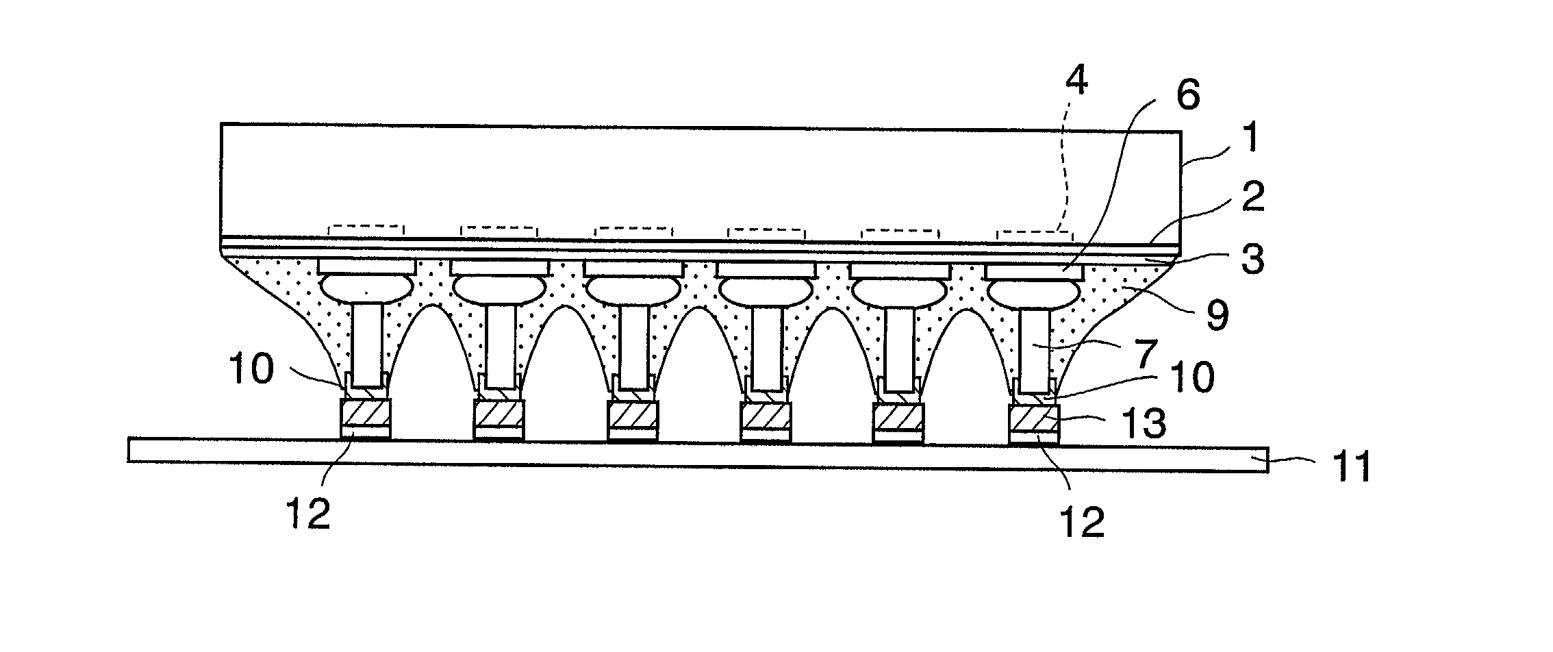
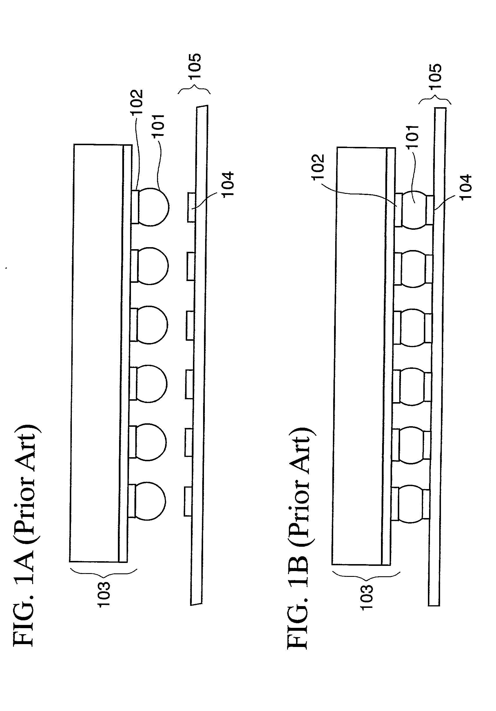
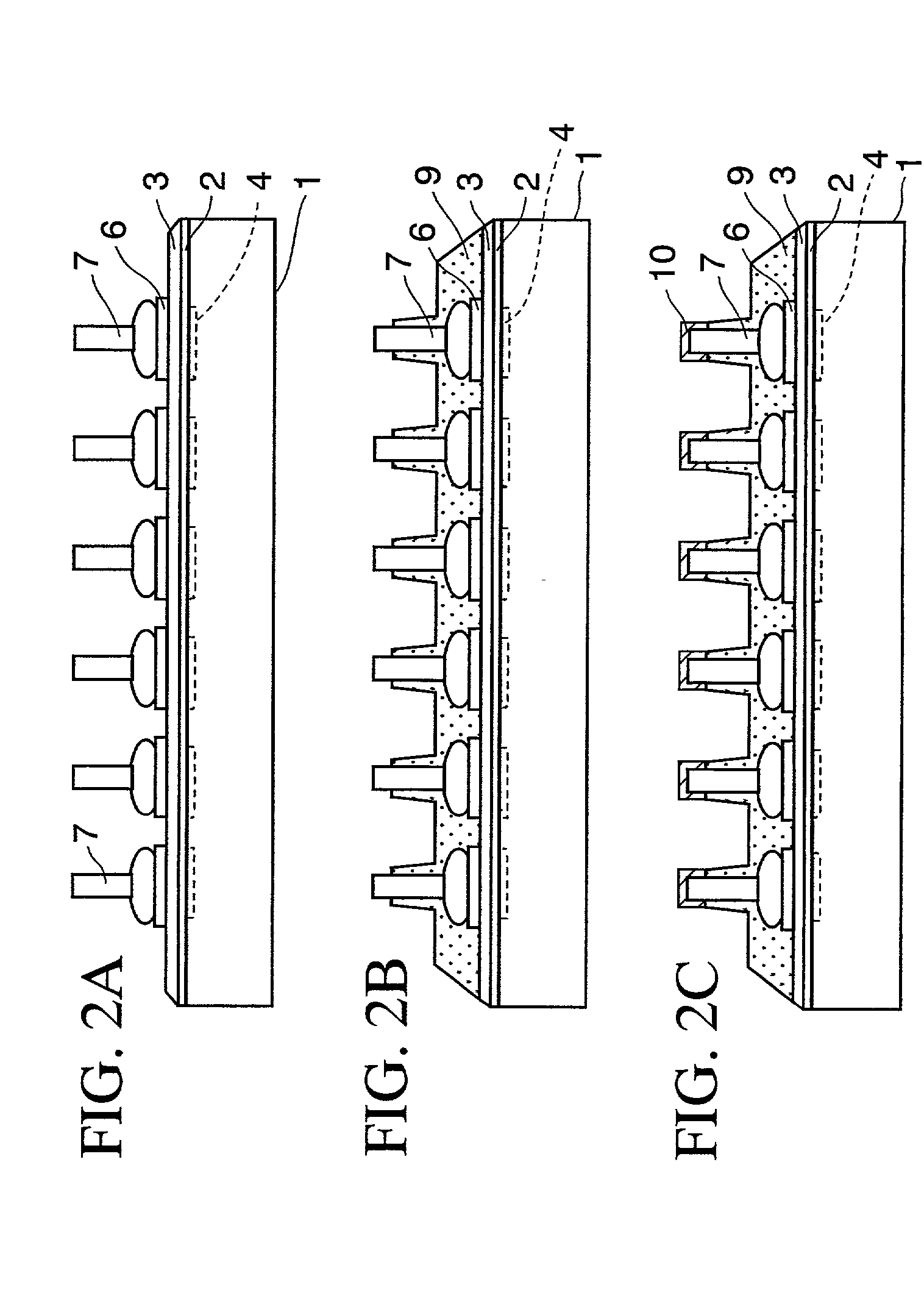
[0029] FIGS. 2A to 2C are sectional views showing steps of covering external terminals of a PGA-type semiconductor device according to a first embodiment of the present invention. FIGS. 3A to 3D are sectional views showing steps of jointing the external terminals to terminals on a mother board. Also, FIG. 4 is a plan view showing relocated wirings of the semiconductor device.

[0030] First, as shown in FIG. 2A, a semiconductor circuit device (substrate) 1 that is formed on a semiconductor substrate such as silicon is prepared. An inorganic insulating film 2 made of SiO.sub.2 and an underlying cover film 3 made of the organic material such as polyimide, benzocyclobutene, etc. are formed in sequence on one surface of the semiconductor circuit device 1.

[0031] Openings 5 for exposing conductive pads (terminals) 4, that are formed on one surface side of the semiconductor circuit device 1, are formed on the inorganic insulating film 2 and the underlying cover film 3...

second embodiment

[0057] (Second Embodiment)

[0058] In FIG. 5A of the first embodiment, the underlying metal layer 8 is formed only on the top ends of the pin-like external terminals 7 of the semiconductor circuit device 1. In this case, the overall pin-like external terminals 7 on the relocated wiring patterns 6 may be covered with the metal layer.

[0059] First, as shown in FIG. 2A, the pin-like external terminals 7 are jointed onto the relocated wiring patterns 6. Then, as shown in FIG. 8A, an underlying metal layer 8X is formed on exposed surfaces of the pin-like external terminals 7 and exposed surfaces of the relocated wiring patterns 6 by the electroless plating method. The underlying metal layer 8X has the multi-layered structure in which the nickel-phosphorus (NiP) layer, the palladium (Pd) layer, and the gold (Au) layer are formed in sequence by the electroless plating method, for example.

[0060] Then, as shown in FIG. 8B, the sealing resin film 9 is formed on the underlying cover film 3. The s...

third embodiment

[0065] (Third Embodiment)

[0066] The top ends of the pin-like external terminals 7 shown in the first and second embodiments are exposed by adjusting the coating of the sealing resin film 9. But the method of exposing the pin-like external terminals 7 is not limited to this. Other examples of the method of exposing the pin-like external terminals 7 will be explained in the following.

[0067] In the third embodiment, as shown in FIG. 9A, the semiconductor circuit device employing the structure in which the pin-like external terminals 7 are directly connected to the conductive pads 4 is prepared in place of the structure in which the pin-like external terminals 7 and the conductive pads 4 are electrically connected via the relocated wiring patterns 6. In addition, the sealing resin film 9 is coated on the underlying cover film 3 to cover perfectly the pin-like external terminals 7, and then the sealing resin film 9 is semi-hardened.

[0068] Then, as shown in FIG. 9B, the sealing resin film...


PUM

PropertyMeasurementUnit
Temperatureaaaaaaaaaa
Flow rateaaaaaaaaaa
Electrical conductoraaaaaaaaaa

Abstract

There are provided a sealing insulating film that is formed on a substrate and melted at a first heating temperature to have a flowability, and external terminals that are formed on the substrate, and connected to other electronic device at a second heating temperature higher than the first heating temperature, and surrounded by the sealing insulating film.

Description

CROSS-REFERENCE TO RELATED APPLICATIONS[0001] This application is based upon and claims priority of Japanese Patent Application No. 2001-351501, filed in Nov. 16, 2001, the contents being incorporated herein by reference.BACKGROUND OF THE INVENTION[0002] 1. Field of the Invention[0003] The present invention relates to an electronic device, an electronic device sealing method and an electronic device connecting method and, more particularly, an electronic device such as a semiconductor device, a wiring substrate, etc. that have external terminals, an electronic device sealing method and an electronic device connecting method.[0004] 2. Description of the Prior Art[0005] With the progress of the miniaturization, the high function, and the high integration of the semiconductor device, the number of input / output terminals tends to increase. Also, in the semiconductor device, there is the request to reduce a size of the package that covers the semiconductor device chip. Under such circums...

Claims


Application Information

Patent Timeline
IPC IPC(8): H01L21/56H01L23/29H01L21/60H01L23/28H01L23/31H01L23/485H05K3/28H05K3/32H05K3/34
CPCH01L23/3114H01L2224/05568H01L2224/131H01L2224/13144H01L2224/13147H01L2224/13164H01L2224/16H01L2924/01004H01L2924/01015H01L2924/01027H01L2924/01029H01L2924/01046H01L2924/01078H01L2924/01079H01L2924/01082H01L2924/3025H05K3/3436H05K2201/0129H05K2201/10977H01L2224/1134H01L2224/05023H01L2924/12042H01L2924/351H01L24/13H01L24/11H01L2224/73104Y02P70/613H01L2224/13H01L2924/01033H01L2924/00013H01L2924/01005H01L2924/01006H01L2924/014H01L2224/11H01L2924/00015H01L2924/00014H01L2224/13099H01L2924/00Y02P70/50H01L23/28
Inventor AIBA, YOSHITAKAMATSUKI, HIROHISASATO, MITSUTAKA
Owner SOCIONEXT INC
Why Eureka
Try Eureka