Method of manufacturing semiconductor wafer

a manufacturing method and technology of semiconductor wafers, applied in the direction of manufacturing tools, grinding machines, lapping machines, etc., can solve the problems of increased quantity of wafer surface to be polished during subsequent double-sided polishing, increased manufacturing equipment, and longer polishing tim

Active Publication Date: 2003-06-05
SUMITOMO MITSUBISHI SILICON CORP
View PDF15 Cites 60 Cited by
  • Summary
  • Abstract
  • Description
  • Claims
  • Application Information

AI Technical Summary

Benefits of technology

[0016] Yet another object of the present invention is to provide a method of manufacturing a semiconductor wafer, in which such a wafer having high level of flatness can be manufactured with a smaller polishing volume in a shorter polishing time, and a back surface of the wafer is not apt to be mirror-polished during the double-sided polishing of the wafer.
[0117] Further, since the occurrence of the nanotopography can be prevented by the double-sided polishing, the decrease in device yield due to the unfavorable deviation of film thickness in the CMP (Chemical Mechanical Polishing) step may also be prevented.

Problems solved by technology

To fabricate a set of equipment for applying the double-sided polishing to those wafers of large gauge, such as 300 mm wafers, disadvantageously the carrier plate and thus the entire unit could be enlarged by a size to accommodate the sun gear.
There has been a problem in this concern that, for example, it may lead to the fabricated equipment for the double-sided polishing that has a diameter not smaller than 3 m.
However, there have been following problems in association with the method for double-sided polishing of the silicon wafers by using the double-sided polisher with no sun gear according to the prior art.
As discussed above, the double-sided polishing method according to the prior art, in which the silicon wafer has been finished to have the same glossiness in both of the front and the back surfaces thereof, could not handle such a case where, for example, only the back surface of the wafer is desired to have a lower glossiness thus to form a satin-finished surface or a case where only the front surface of the wafer is desired to be mirror-polished in order to form only the back surface of the wafer into a gettering surface.
As the damage is greater, the quantity to be polished off from the surface of the wafer during subsequent double-sided polishing is increased.
If the quantity of polishing is greater than 10 .mu.m, problematically the polishing time may be longer and additionally there will be a fear that the back surface is polished excessively thus to form a complete mirror surface.
Further, the quantity of polishing lower than 0.5 .mu.m in the back surface of the wafer will be insufficient to provide an effect on reducing the roughness in the back surface.
Further, with the quantity of polishing greater than 1.5 .mu.m, disadvantageously, identifying of the front surface and the back surface based on the mirror-finished condition is no more effective.

Method used


Image

  • Method of manufacturing semiconductor wafer
  • Method of manufacturing semiconductor wafer
  • Method of manufacturing semiconductor wafer

Examples


first embodiment

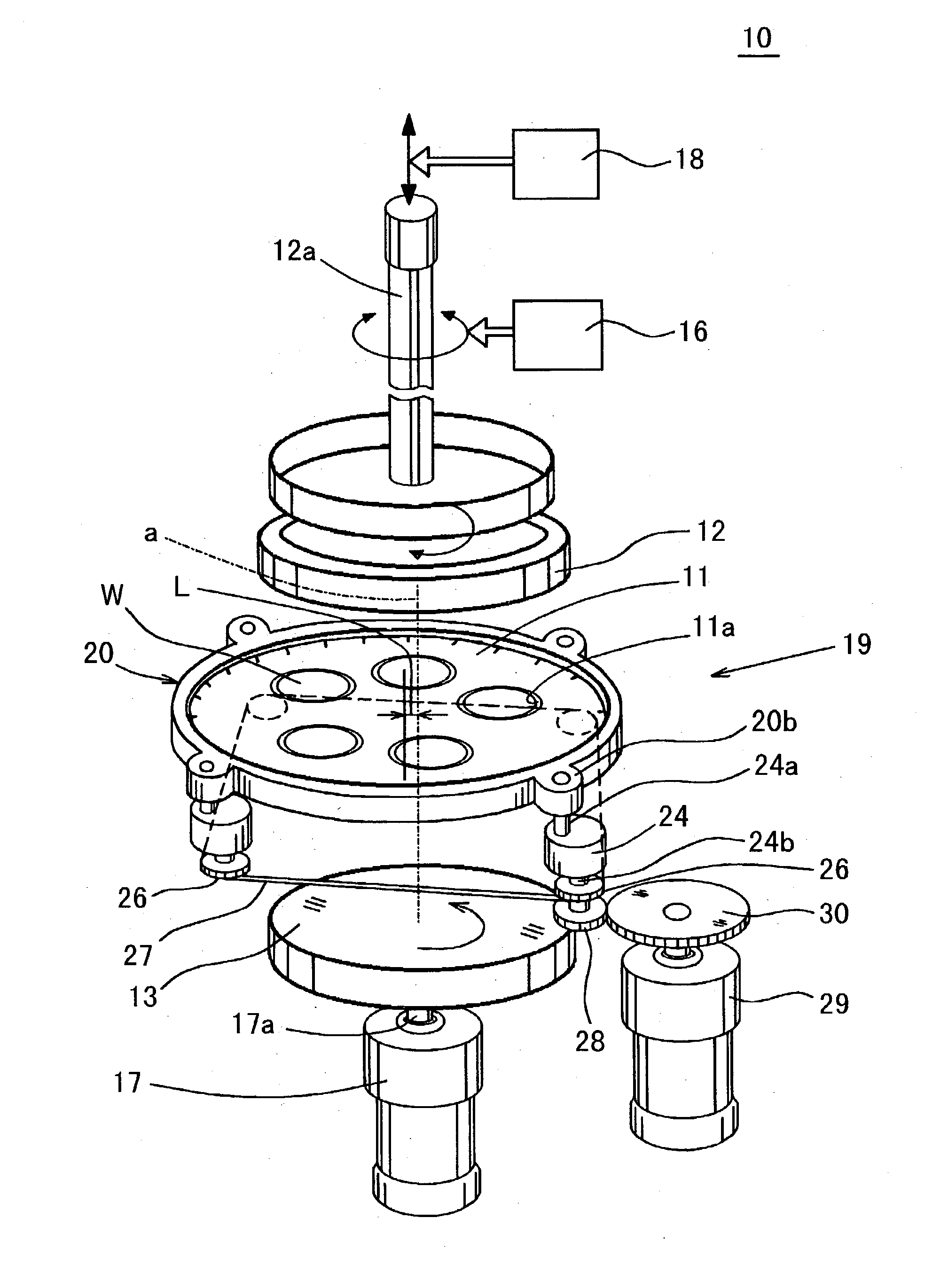
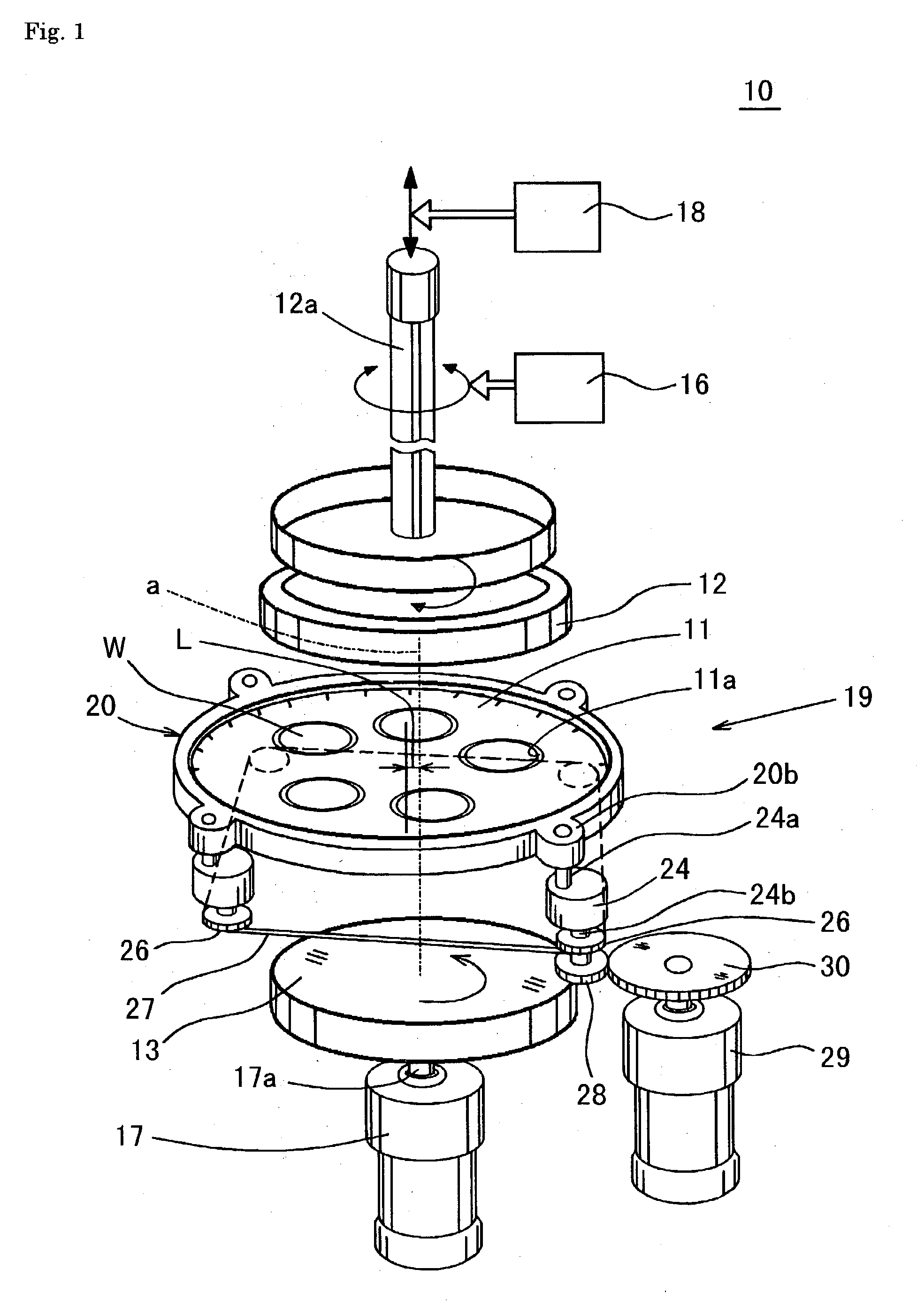
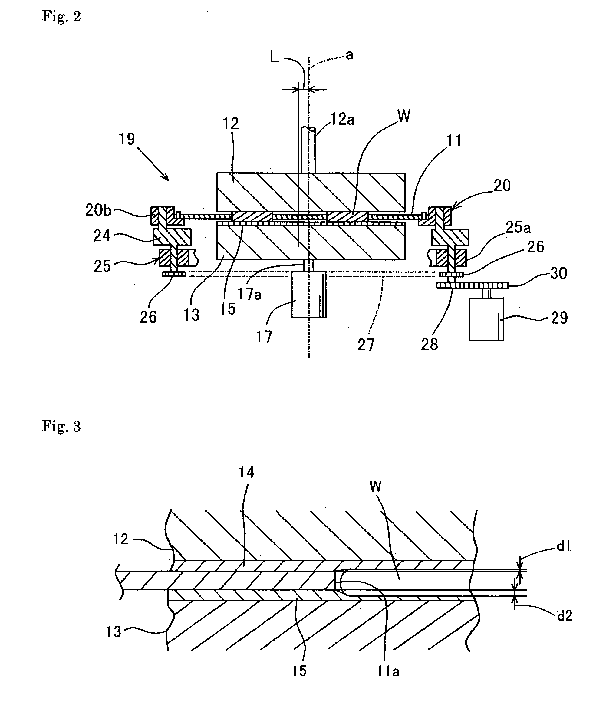
[0135] In FIG. 1 and FIG. 2, reference numeral 10 generally designates a double-sided polisher used in a method of manufacturing a semiconductor wafer according to the present invention. This double-sided polisher 10 comprises a carrier plate 11 made of epoxy-glass having a circular disc-like shape in plan view in which five of wafer holding holes 11a have been formed by every 72 degrees (in the circumferential direction) around an axis line of the plate so as to penetrate through the plate, and a pair of upper surface plate 12 and lower surface plate 13 functioning for clamping silicon wafers "W", each having a diameter of 300 mm and having inserted and thus held operatively in the wafer holding hole 11a so as to be free to rotate therein, from above and below sides with respect to the wafers W and also functioning for polishing the surfaces of the wafers W by moving themselves relatively with respect to the silicon wafers W. The carrier plate 11 is disposed between the upper surfa...

second embodiment

[0162] Referring now to FIG. 7, a method of manufacturing semiconductor wafer according to the present invention will now be described.

[0163] As shown in FIG. 7, this second embodiment is representative of an example that has employed, instead of the hard expanded urethane foam pad 14 extended over the upper surface plate 12 in the first embodiment, a hard plastic plate 40 which allows almost no slurry to attach to the surface thereof.

[0164] This configuration allows, during polishing process, exclusively the front surface of the silicon wafer W to sink into the soft non-woven fabric pad 15 at a sink rate of d2 and thus to be mirror-polished, while the back surface of the silicon wafer W, which is engaged with the hard plastic plate 40, may not be polished at all. By way of this, the silicon wafer may be finished with the waviness (nanotopography) created by the acid etching left in the back surface as it was.

[0165] Other description on configuration, operation and effect of this em...

third embodiment

[0166] A method of manufacturing a semiconductor wafer according to the present invention will now be described.

[0167] In the third embodiment, the polishing cloths extended over the upper surface plate 12 and the lower surface plate 13, as used in the first embodiment shown in FIG. 1, are specified as the same soft non-woven fabric pads 15, in which the upper surface plate 12 is driven by the upper rotary motor 16 to rotate at a lower speed (5 rpm), while the lower surface plate 13 is driven by the lower rotary motor 17 to rotate at a higher speed (25 rpm) to carry out a double-sided polishing. At that time, the slurry is supplied at a rate of 2.0 litter / min, and the quantity to be polished off from the front surface of the wafer is 10 .mu.m and that from the back surface of the wafer is equal to or less than 1 .mu.m.

[0168] With this arrangement, different polishing rates are created between the front and the back surfaces of the wafer, which in turn brings a difference in glossine...


PUM


Abstract

An object of the present invention is to provide a semiconductor wafer having a front and a back surfaces polished so as to have different glossiness from each other, yet with a lower cost. The glossiness of the front surface and the back surface can be selected arbitrarily. In a double-sided polisher with no sun gear, silicon wafers W are inserted in respective holding holes 11a of a carrier plate 11. The wafers W are placed with their back surfaces facing up. An expanded urethane foam pad 14 is pressed against the back surfaces of the wafers W and a non-woven fabric pad 15 is pressed against the front surfaces of the wafers W. A carrier holder 20 and thus the carrier plate 11 are then driven to make a circular motion associated with no rotation on their own axes within a horizontal plane while supplying a slurry to the wafers W from an upper surface plate 12 side. As a result, each of the front and the back surfaces of respective silicon wafers W can be polished uniformly over entire area thereof respectively. At that time, the urethane pad 14 has a sink rate of the wafer lower than that of the non-woven fabric pad 15. Therefore, such a polished wafer having the back surface formed into a satin-finished surface and the front surface formed into a mirror-finished surface can be obtained. Alternatively, those polishing cloths having different sink rates from each other may be employed for the upper and the lower surface plates, respectively. Further, the upper surface plate and the lower surface plate may be rotated at different speeds from each other. Those methods are also advantageously used to manufacture the semiconductor wafer having different glossiness between the front surface and the back surface thereof.

Description

[0001] The present invention relates to a method of manufacturing a semiconductor wafer, and in more specific, to a method of manufacturing a semiconductor wafer in which the semiconductor wafer is polished by using a double-sided polisher having no sun gear incorporated thereinto, thereby obtaining such a semiconductor wafer with a front and a back surfaces having a different glossiness from each other.DESCRIPTION OF THE PRIOR ART[0002] In manufacturing wafers having both surfaces polished according to the prior art, such a process has been employed as described below. In specific, a single crystal silicon ingot is sliced to be formed into silicon wafers, and then those silicon wafers are subjected to a series of processing steps of beveling, lapping and acid etching in sequence. These steps are followed by a double-sided polishing process for mirror-finishing both front and back surfaces of the wafers.[0003] This double-sided polishing typically uses a double-sided polisher having...

Claims


Application Information

Patent Timeline
Patent Type & Authority Applications(United States)
IPC IPC(8): B24B37/04B24B37/08B24B37/24B24B37/28
CPCB24B37/042B24B37/28B24B37/24B24B37/08H01L21/304
Inventor TANIGUCHI, TORUMORITA, ETSUROMATAGAWA, SATOSHIHARADA, SEIJIONO, ISOROKUENDO, MITSUHIROYOSHIDA, FUMIHIKO
Owner SUMITOMO MITSUBISHI SILICON CORP
Why Eureka
Try Eureka