

Organic electroluminescent device with a containing fluorine inorganic layer
an electroluminescent device and organic technology, applied in the direction of electric lighting sources, solid-state devices, electric light sources, etc., can solve problems such as dealing with interfaces
- Summary
- Abstract
- Description
- Claims
- Application Information
AI Technical Summary
Benefits of technology
Problems solved by technology
Method used
Image

Examples
example 2
Device 2
[0024] Wash an ITO glass substrate as follows: firstly, wash it with detergent, place it in an ultrasonic vessel be vibrated using pure water and isopropyl alcohol twice, respectively, and then dry it in an oven. After drying, place an ITO glass substrate on the carrier plate, place in the chamber for the plasma treatment.
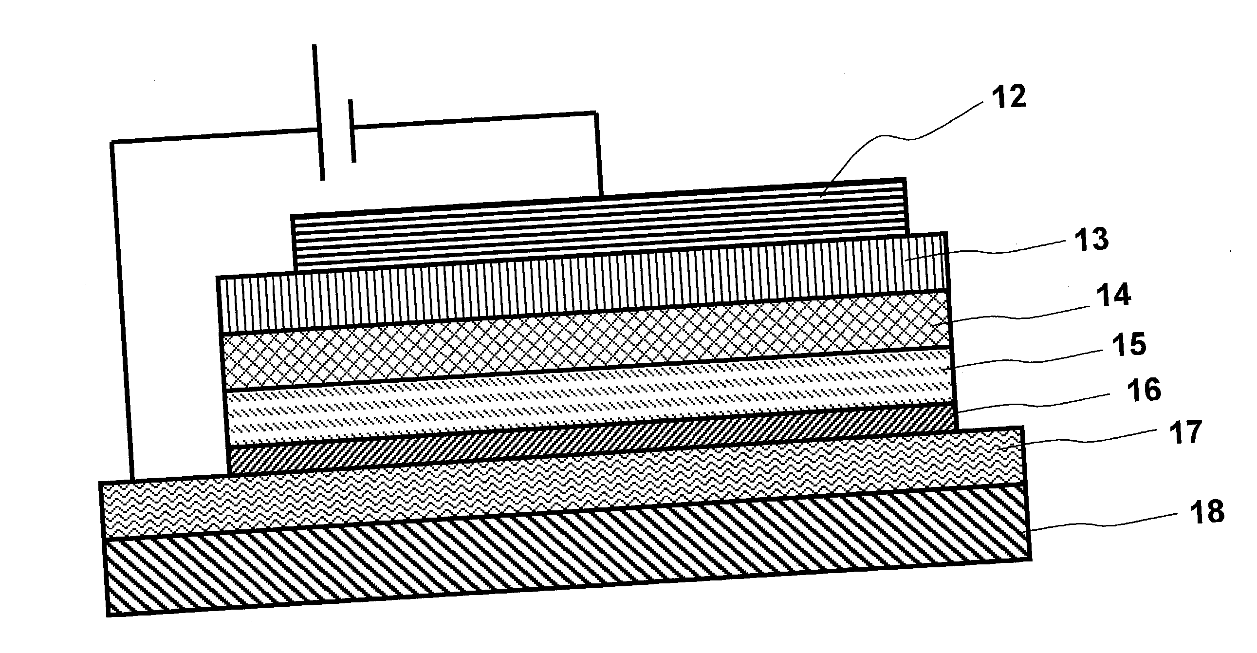
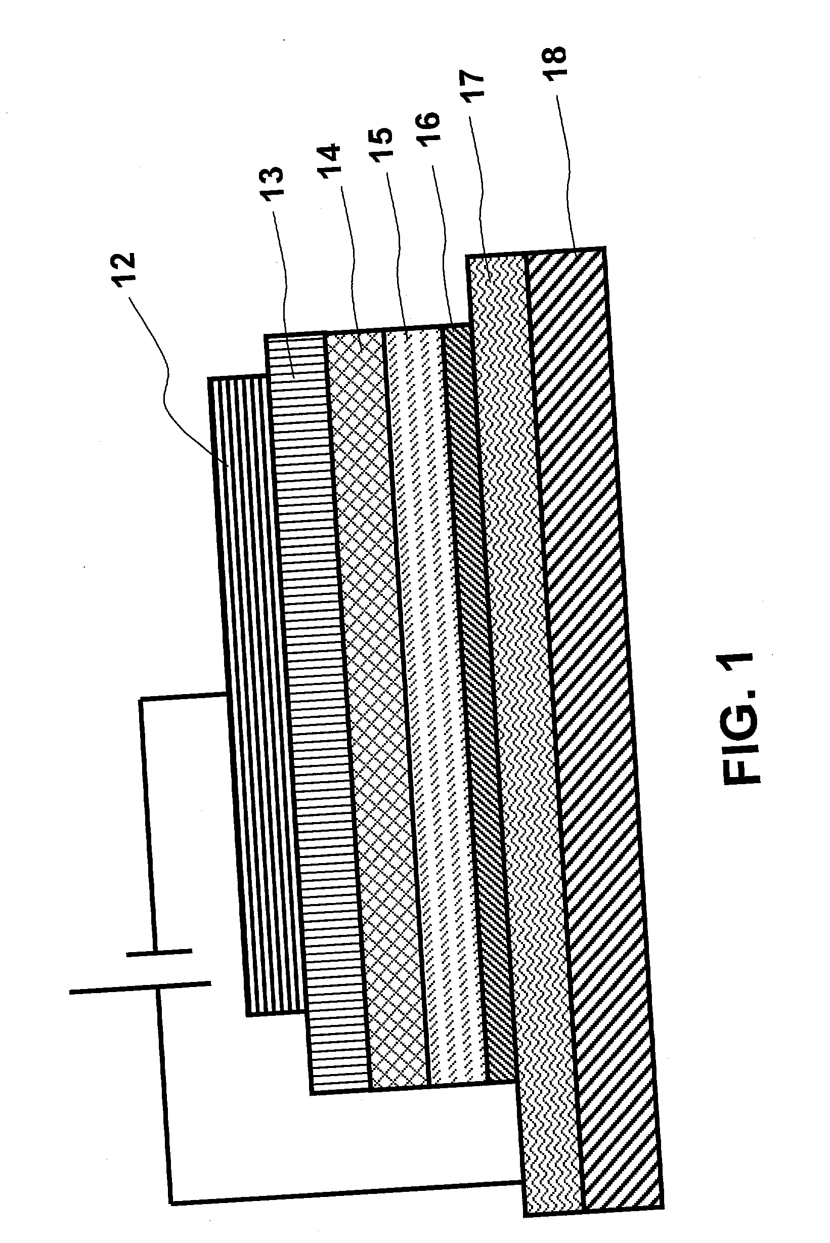
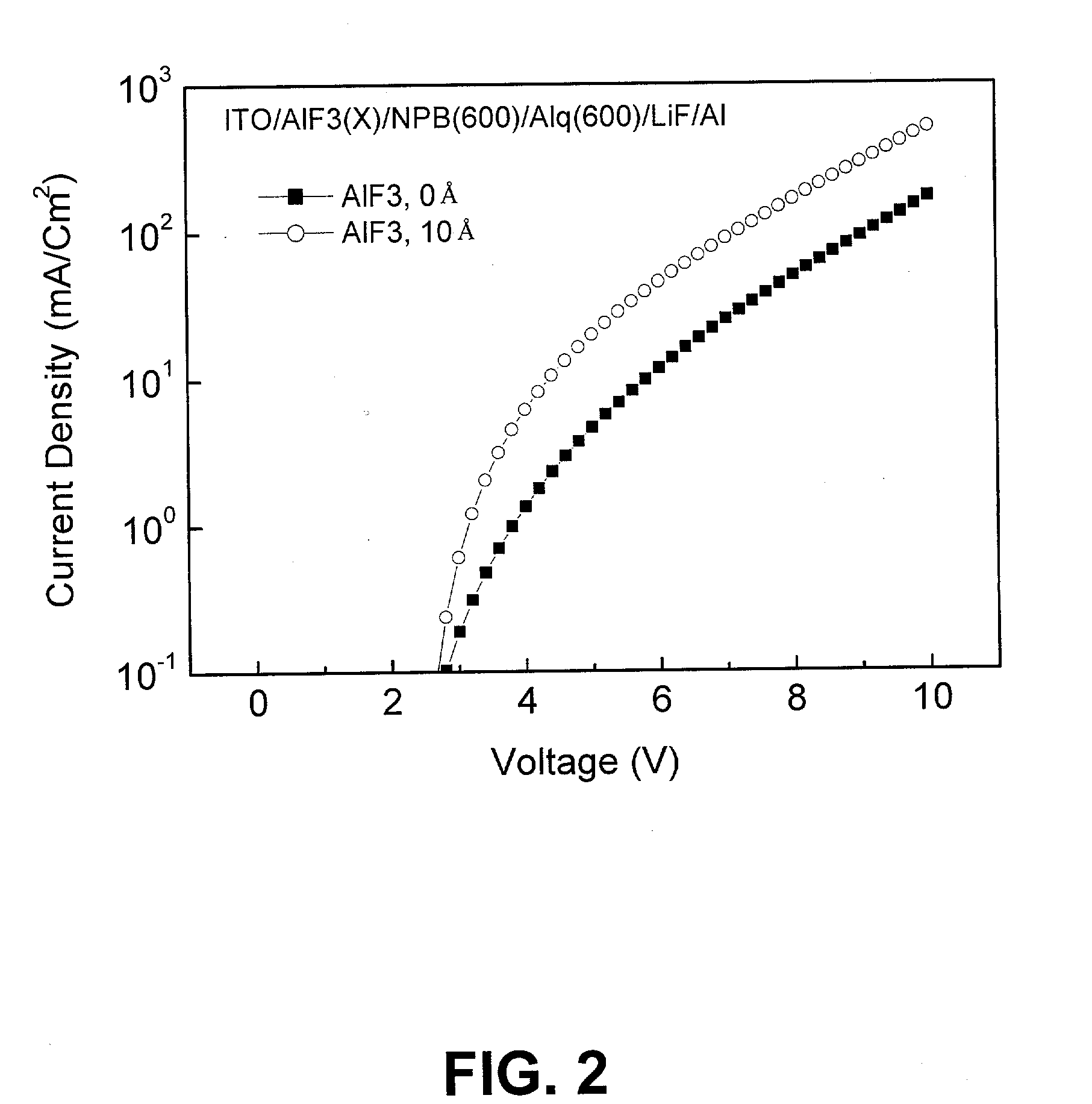
[0025] Firstly, on an ITO glass substrate sequentially it is evaporated with AlF3 (10 A), a hole-transport layer, NPB (600 A), an organic light-emitting layer / an electron-transport layer, Alq (600 A), LiF (5 A), and Al (1000 A) as a cathode metallic electrode. After finish the device fabrication place it in the dry box for the package and the device property test. An initial voltage of the device is 2.6 V, at 10 V the current density and brightness is 507 mA / cm2 and 8697 cd / m2, respectively. The highest efficiency of the device is 2.8 lm / W. FIG. 2 and FIG. 3 illustrate the current density and brightness of the device 2 are higher than those of the device 1....
example 3
Device 3
[0026] Wash an ITO glass substrate as follows: firstly, wash it with detergent, place it in an ultrasonic vessel be vibrated using pure water and isopropyl alcohol twice, respectively, and then dry it in an oven. After drying, place an ITO glass substrate on the carrier plate, place in the chamber for the plasma treatment. Firstly, on an ITO glass substrate sequentially it is evaporated with AlF3 (30 A), a hole-transport layer, NPB (600 A), an organic light-emitting layer / an electron-transport layer, Alq (600 A), LiF (5 A), and Al (1000 A) as a cathode metallic electrode. After finish the device fabrication place it in the dry box for the package and the device property test. An initial voltage of the device is 2.6 V, and the highest efficiency of the device is 3.2 lm / w.
example 4
Device 4
[0027] Wash an ITO glass substrate as follows: firstly, wash it with detergent, place it in an ultrasonic vessel be vibrated using pure water and isopropyl alcohol twice, respectively, and then dry it in an oven. After drying, place an ITO glass substrate on the carrier plate, place in the chamber for the plasma treatment.
[0028] Firstly, on an ITO glass substrate sequentially it is evaporated with AlF3 (50 A), a hole-transport layer, NPB (600 A), an organic light-emitting layer / an electron-transport layer, Alq (600 A), LiF (5 A), and Al (1000 A) as a cathode metallic electrode. After finish the device fabrication place it in the dry box for the package and the device property test. An initial voltage of the device is 2.6 V, and the highest efficiency of the device is 2.9 lm / W. FIG. 5 is a comparative lifetime for the device 1 and the device 4, at 20 mA / cm2 of the constant current density the brightness for two devices is about 600 cd / m2, FIG. 5 indicates the brightness decay...
PUM
 Abstract
Description
Claims
Application Information