Semiconductor device and manufacturing method for the same

Active Publication Date: 2003-09-18
TESSERA ADVANCED TECH
View PDF6 Cites 95 Cited by
  • Summary
  • Abstract
  • Description
  • Claims
  • Application Information

AI Technical Summary

Problems solved by technology

However, as mentioned above, when a wiring line and a connection plug are formed of copper by the dual damascene method, a production yield of the semiconductor device is so low that the semiconductor device can not be produced stably.
The cavity causes a connection defect between the connection plug and the wiring line, the decrease of the production yield of the semiconductor device and an unstable operation of the semiconductor device as the result of a long-term use.
However, when the connection plug was formed in a part (301b) which was not a boundary, the cavity was difficult to be generated around the lower portion of the connection plug.
Especially, it was found that the cavity was easy to be generated in a region where the boundaries of the plurality of grains overlap complicatedly.
This causes cavities.
When an oxide film exists on the copper containing metal film of the first wiring line, it is difficult to form the silicide layer in a region where the oxide film is formed.
As a result, when the forming process of the silicide layer is carried out in the condition that the oxide film is adhered to the surface of the first wiring line, the thickness of the silicide layer is not uniform.
As a result, the metal silicide layer cannot have a uniform thickness.
When the oxide film with un-uniform thickness has been formed on the copper containin

Method used


Image

  • Semiconductor device and manufacturing method for the same
  • Semiconductor device and manufacturing method for the same
  • Semiconductor device and manufacturing method for the same

Examples


first embodiment

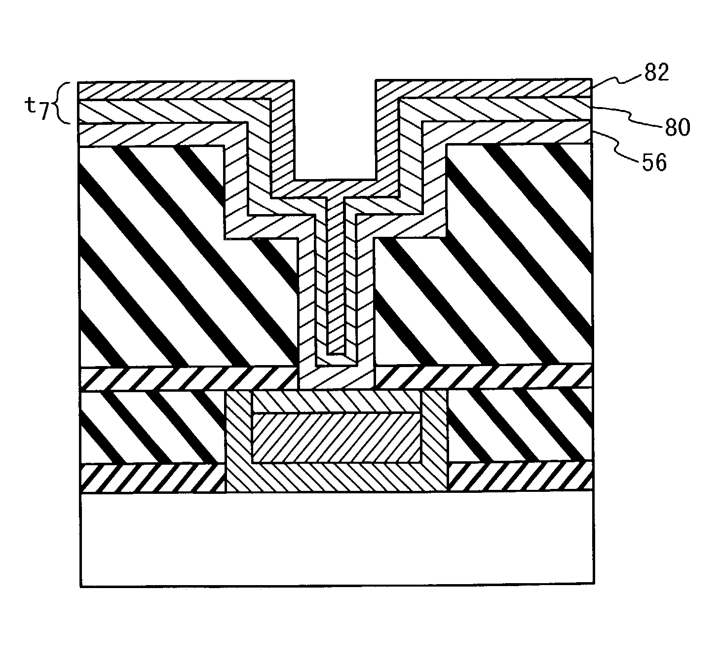
[0157] FIG. 3 is a cross sectional view showing the wiring line structure in the present invention. A first laminate layer 14a in which a first SiCN film 12, L-Ox film and a SiO.sub.2 film are laminated in this order, and a second laminate layer 14b in which a second SiCN film 16, a silicon oxide film 18, a third SiCN film 20 and a L-Ox film and a SiO.sub.2 film are laminated are laminated on an insulating film 106 on the silicon substrate (not shown). In the first laminate layer 14a and the second laminate layer 14b, the first copper wiring line 22a and the second copper wiring line 22b are formed, respectively.

[0158] The first copper wiring line 22a are formed of a tantalum-based barrier metal film 24a and a copper film 26a. In the silicon oxide film 18, a connection plug 28 is formed to connect with the surface of the first copper wiring line 22a. The connection plug 28 is formed of a tantalum-based barrier metal film 30 and a copper film 32. In the second laminate layer 14b, the...

embodiment 2

[0173] The second embodiment is different from the first embodiment in that BTA is evaporated and removed through a heating process at about 350 C instead of the ammonia plasma process, before the siliciding process of the surface of the copper film 26a and the surface of the copper film 26b. Through the heating process, the wiring line structure shown in FIG. 3 is formed. It should be noted that the heating temperature at which BTA is evaporated and removed may be from 150 C to 450 C. By the fluorescence X ray analysis of the formed wiring line structure, the existence of CuSix is confirmed.

[0174] By carrying out the ammonia plasma process for the evaporation and removal of the BTA as in the first embodiment, the siliciding process can be carried out while BTA is removed. Therefore, it is possible to control the siliciding process such as a film thickness control of the Cu silicide. Also, by carrying out the heating process for the evaporation and removal of the BTA as in the secon...

embodiment 3

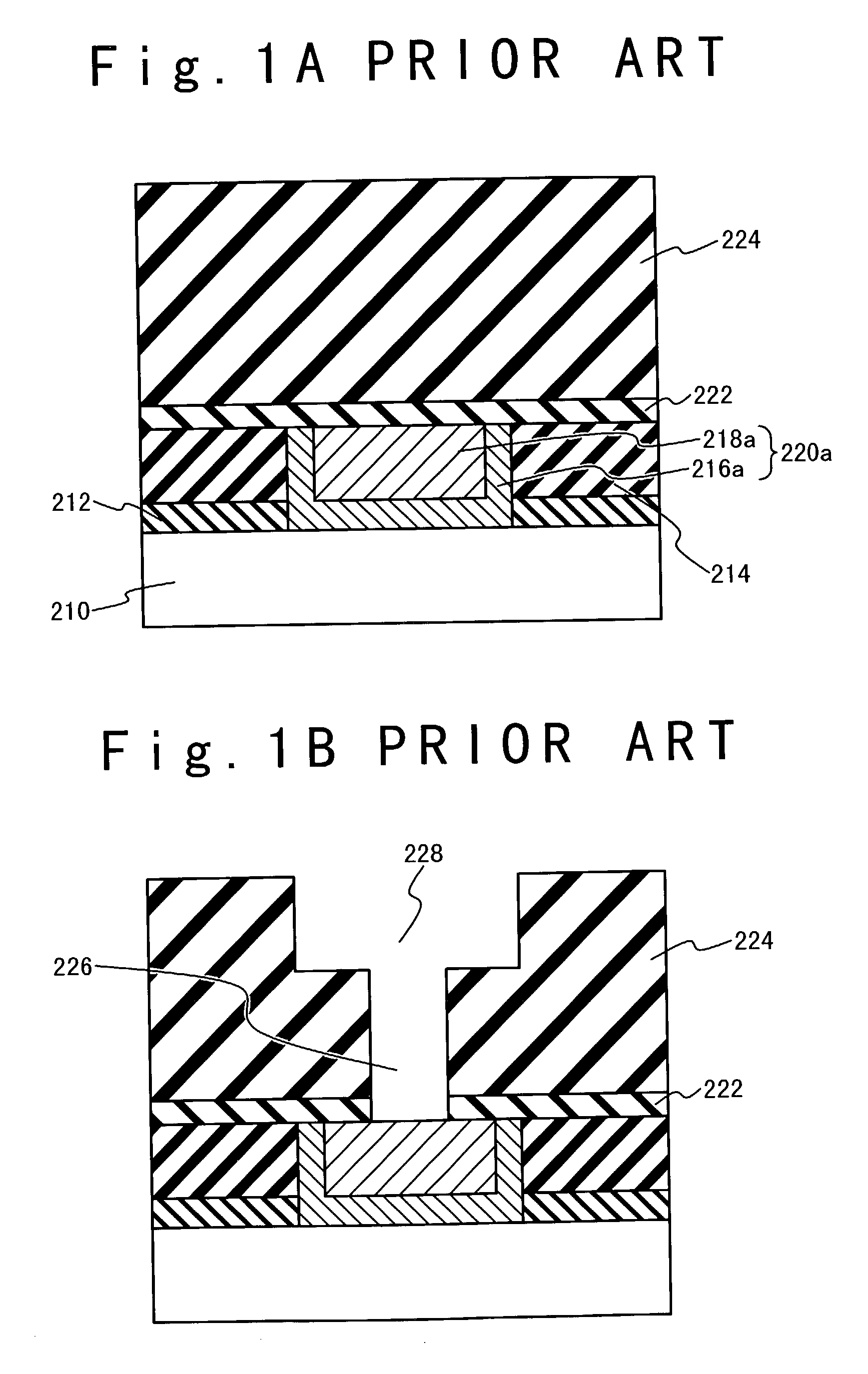
[0175] FIG. 5 is a diagram showing the wiring line structure in the third embodiment. The third embodiment is different from the first embodiment in that the first Cu silicide layer 34a and the second Cu silicide layer 34b are not formed, and that the BTA anti-corrosion processing is not carried out. The description of the same components of FIG. 5 as those of FIG. 3 will be omitted by allocating the same reference numerals.

[0176] In the third embodiment, the processes are carried out as in the first embodiment until the CMP process to the copper film 26a of the first copper wiring line 22a process. Subsequently, the second SiCN film 16 and the silicon oxide film 18 are formed without carrying out the siliciding process of the surface of the copper film 26a. Before the second SiCN film 16 is formed, a surface treat process of the copper film 26a of the first copper wiring line 22a is carried out by the ammonia plasma process. The process after the silicon oxide film 18 is formed is ...


PUM


Abstract

In a method of manufacturing a semiconductor device, a first wiring line composed of a copper containing metal film is formed on or above a semiconductor substrate. A first interlayer insulating film is formed on a whole surface of the semiconductor substrate to cover the first wiring line. The first interlayer insulating film is selectively removed to form a connection hole reaching the first wiring line. A barrier metal film is formed to cover an inner surface of the connection hole and then a copper containing metal film is formed to fill the connection hole. The copper containing metal film formed outside the connection hole is removed. A second interlayer insulating film is formed on a whole surface of the semiconductor substrate to cover the copper containing metal film formed in the connection hole. The second interlayer insulating film is selectively removed to form a wiring line groove such that the copper containing metal film formed in the connection hole is exposed at a bottom. A barrier metal film is formed to cover an inside of the wiring line groove and then a copper containing metal film is formed to fill the wiring line groove. Then, the copper containing metal film outside the wiring line groove is removed to form a second wiring line.

Description

[0001] 1. Field of the Invention[0002] The present invention relates to a semiconductor device and a manufacturing method for the same. More particularly, the present invention relates to a semiconductor device containing a copper containing metal wiring line and a manufacturing method for the same[0003] 2. Description of the Related Art[0004] In recent years, a low resistance material such as copper is used as a wiring line material for demand of the high speed operation of a semiconductor device.[0005] As a damascene process for forming a copper wiring line structure, a single damascene method and a dual damascene method are known. In the single damascene method, only a wiring line is formed by the damascene process. In the dual damascene method, a wiring line groove is embedded with copper in addition to a connection hole, to form the connection plug and the wiring line. Conventionally, in the single damascene method, the connection plug is formed of a refractory metal such as tu...

Claims


Application Information

Patent Timeline
IPC IPC(8): H01L21/02H01L21/285H01L21/3205H01L21/321H01L21/3213H01L21/768H01L23/52H01L23/522H01L23/532
CPCH01L21/02068H01L21/02074H01L2924/0002H01L21/2855H01L21/32136H01L21/76802H01L21/76807H01L21/76838H01L21/76877H01L21/76889H01L23/5226H01L23/53238H01L23/53295H01L2924/00H01L21/76883H01L21/76849H01L21/28
Inventor HIRONAGA, NOBUOTAKEWAKI, TOSHIYUKIKUNISHIMA, HIROYUKIYAMAMOTO, YOSHIAKI
Owner TESSERA ADVANCED TECH
Why Eureka
Try Eureka