Display device and method for making the same

a technology of display units and display units, applied in the direction of discharge tubes/lamp details, organic semiconductor devices, discharge tubes luminescent screens, etc., can solve the problems of increased production costs, increased power consumption of display units, and reduced brightness half-life,

Inactive Publication Date: 2003-09-18
SONY CORP
View PDF7 Cites 15 Cited by
  • Summary
  • Abstract
  • Description
  • Claims
  • Application Information

AI Technical Summary

Problems solved by technology

Unfortunately, a large current in the organic EL device accelerates deterioration of the organic layer, resulting in a decrease in lifetime (brightness half-life) and an increased in power consumption of the display unit.
However, this method has the following disadvantages: The method requires an additional step for forming the buffer layer on the organic layer, resulting in an increase in production cost and a complicated display unit structure.
Furthermore, the buffer layer of the resulting display unit absorbs light of a specific wavelength range; hence, the display unit does not have desired light-emitting characteristics in this specific wa

Method used


Image

  • Display device and method for making the same
  • Display device and method for making the same
  • Display device and method for making the same

Examples


Embodiment Construction

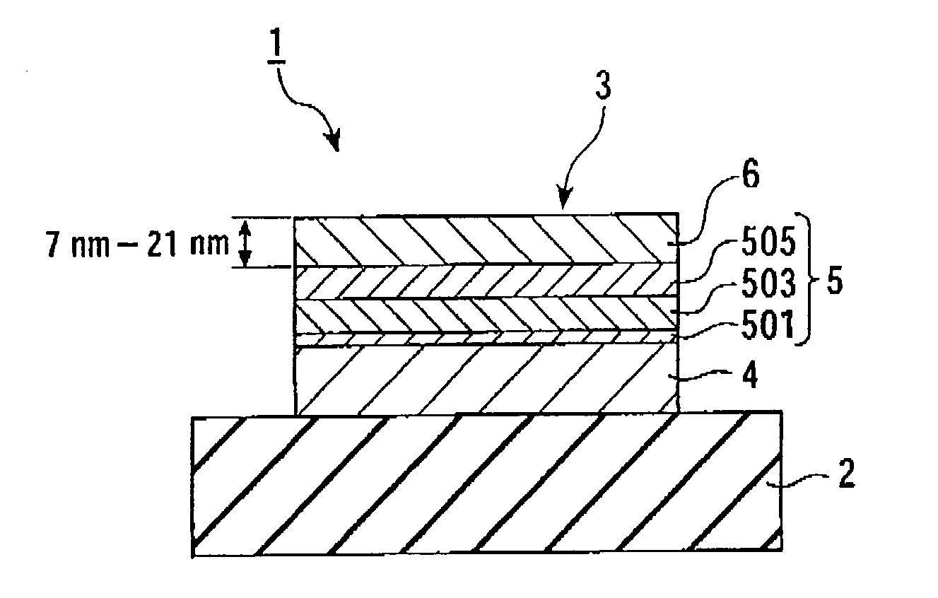
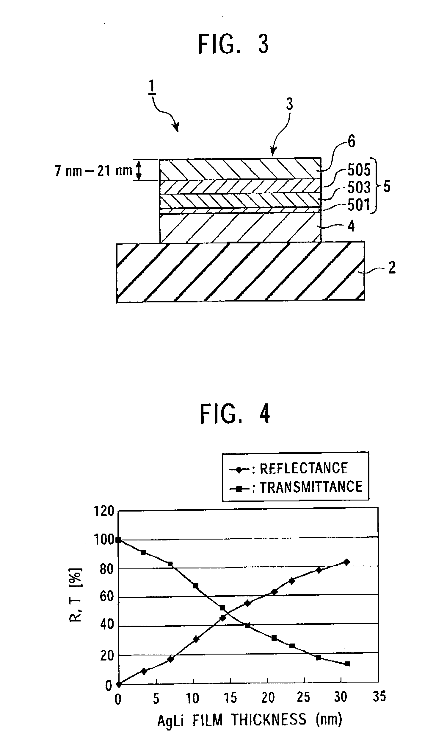
[0042] With reference to FIG. 2, a chromium lower electrode 4 was formed into a thickness of 200 nm on an inner surface of a glass substrate 2 with a thickness of 0.7 mm by a DC magnetron sputtering process. The surface of the lower electrode 4 was exposed to an oxygen plasma for 30 seconds to form a chromium oxide layer on the lower electrode 4.

[0043] The substrate 2 was transferred into an organic deposition chamber through a vacuum system at 10.sup.-4 Pa without exposing the substrate 2 to air. While the chamber was being evacuated to about 3.times.10.sup.-5 Pa, 2-TNATA [4,4',4"-tris(2-naphtylphenylamino)triphenylamine] was deposited into a thickness of 30 nm, an .alpha.-NPD [4,4'-bis(N-(1-naphthyl)-N-phenylamino)biphenyl] was deposited into a thickness of 20 nm, and then an Alq.sub.3 [tris(8-quinolinolato)aluminum(-III)] containing coumarin 6 was deposited into a thickness of 30 nm.

[0044] The substrate 2 was transferred into another deposition chamber for forming a cathode throu...


PUM


Abstract

A top-emitting display unit is fabricated by the following steps: A lower electrode is formed on a substrate. An organic layer including a luminescent sublayer is formed on the lower electrode. Furthermore, an upper electrode containing lithium is formed by a sputtering process into a thickness of 7 nm to 21 nm. The upper electrode functions as a cathode. The lithium content in the upper electrode is in the range of 0.3 to 1.9 percent by weight. In the sputtering process, the upper electrode is preferably formed at a deposition rate of 50 nm/min or less.

Description

[0001] 1. Field of the Invention[0002] The present invention relates to display units and methods for making the same. In particular, the present invention relates to a display unit including a luminescent device that has an organic layer between electrodes and relates to a method for making the same.[0003] 2. Description of the Related Art[0004] A typical organic electroluminescent (EL) device based on electroluminescence of an organic material has an organic layer that includes an organic hole transport sublayer and an organic luminescent sublayer between an anode and a cathode. The organic EL device has attracted attention as a high-brightness luminescent device that can be driven by low DC voltage. The organic EL device has a structure including a substrate, a lower electrode functioning as the anode or cathode on the substrate, the organic layer including the luminescent sublayer on the lower electrode, and an upper electrode functioning as the cathode or anode. The light emerg...

Claims


Application Information

Patent Timeline
IPC IPC(8): H01L51/50H01L51/52H05B33/10H05B33/26
CPCH01L51/5221H01L2251/5315H01L51/5234H10K50/828H10K2102/3026H05B33/10
Inventor SHIBASAKI, TAKANORIHIRANO, TAKASHIMORI, TAKAOYAMADA, JIRO
Owner SONY CORP
Why Eureka
Try Eureka