Ridge-waveguide semiconductor laser device

a laser device and semiconductor technology, applied in lasers, laser optical resonator construction, laser details, etc., can solve the problems of increasing the oscillation threshold current, operating speed characteristics, and not improving the temperature characteristics sufficiently

Inactive Publication Date: 2003-09-25
MITSUBISHI ELECTRIC CORP
View PDF8 Cites 15 Cited by
  • Summary
  • Abstract
  • Description
  • Claims
  • Application Information

AI Technical Summary

Problems solved by technology

This large resistance causes the heat generation and the large RC time constant, which offers a disadvantage in improving the temperature characteristics and the operating speed characteristics.
However, in reality, the temperat...

Method used


Image

  • Ridge-waveguide semiconductor laser device
  • Ridge-waveguide semiconductor laser device
  • Ridge-waveguide semiconductor laser device

Examples


first embodiment

[0021] First Embodiment

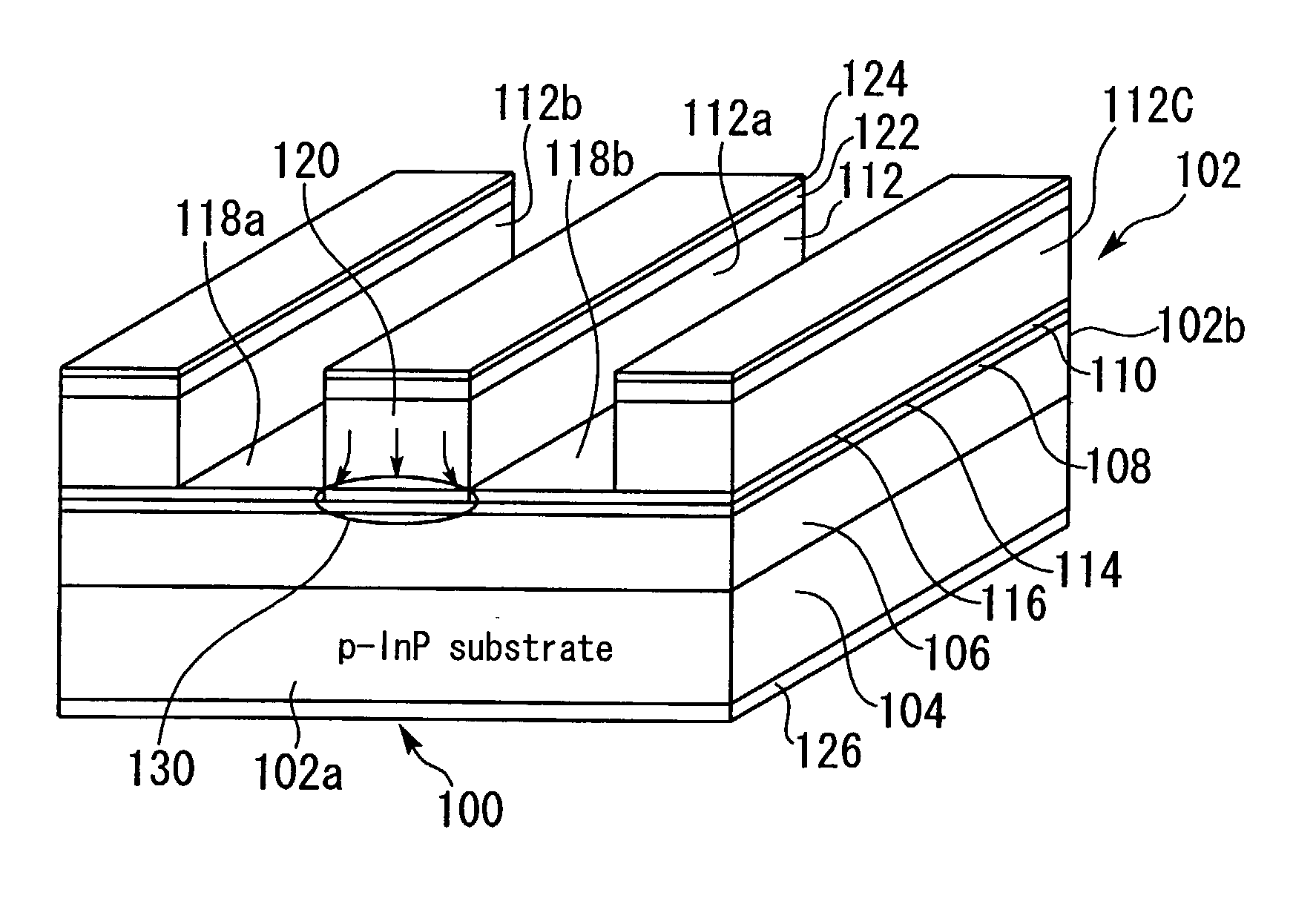
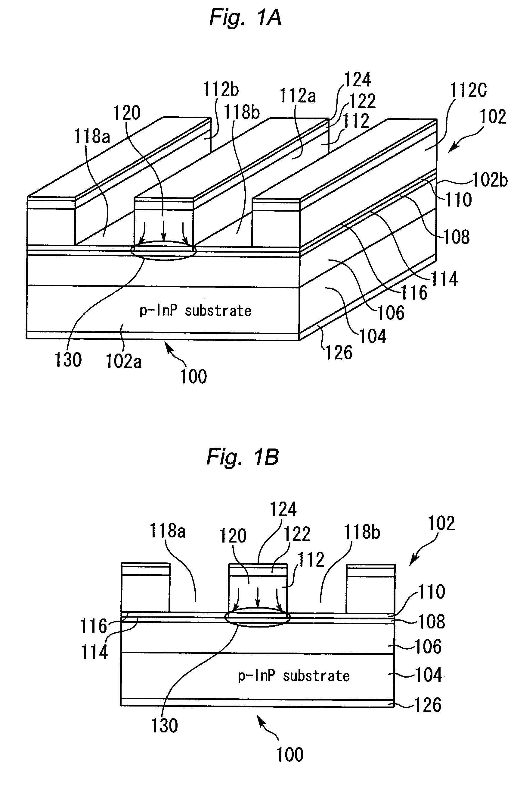
[0022] FIGS. 1A and 1B are views showing a ridge-waveguide semiconductor laser device according to a first embodiment of the present invention. FIG. 1A is a perspective view thereof and FIG. 1B is a cross-sectional view thereof.

[0023] The first embodiment is a ridge-waveguide semiconductor laser device 100 that uses the p-type semiconductor substrate. The ridge-waveguide semiconductor laser device 100 has a double hetero-structure element 102. The double hetero-structure element 102 includes a pair of mutually opposing facets 102a, 102b, and is constructed using a p-type semiconductor substrate 104. The semiconductor substrate 104 is, for example, a square p-type InP substrate having a thickness of 250 to 350 .mu.m. On all over the upper surface of the semiconductor substrate 104, a p-type InP cladding layer 106 is deposited to a thickness of 1 to 2 .mu.m.

[0024] On all over the upper surface of the cladding layer 106, an active layer such as an AlGaInAs-based ...

second embodiment

[0037] Second Embodiment

[0038] FIG. 2 is a cross-sectional view showing the ridge-waveguide semiconductor laser device according to a second embodiment of the present invention. The laser device in the second embodiment has high-resistance regions 132 resulting from lattice defect in the portions exposed at the bottoms of the stripe-like trenches 118a and 118b of the first cladding layer 110. The device according to the second embodiment has almost the same structure as the device in the first embodiment except the above-mentioned point. Any part corresponding to a counterpart of the first embodiment is designated by the same reference number as the first embodiment.

[0039] The high-resistance regions 132 are formed by implanting ions of an inactive element such as H (hydrogen), He (helium) or Ar (argon) from the stripe-like trenches 118a, 118b toward the first cladding layer 110. In this ion implantation process, acceleration energy of ions is set to such a degree that neither impla...

third embodiment

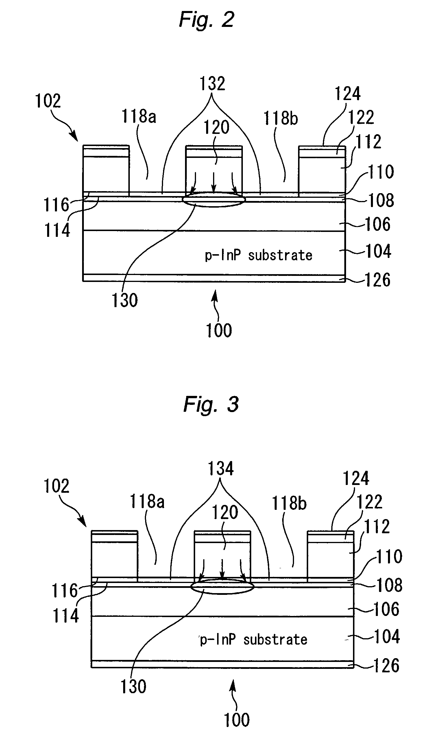
[0041] Third Embodiment

[0042] FIG. 3 is a cross-sectional view showing a ridge-waveguide semiconductor laser device according to a third embodiment of the present invention. The laser device in the third embodiment has high-resistance regions resulting from introduction of F (fluorine) to the portions exposed at the bottoms of the stripe-like trenches 118a and 118b of the first cladding layer 110. The device according to the third embodiment has almost the same structure as the device in the first embodiment except the above-mentioned point. Any part corresponding to a counterpart of the first embodiment is designated by the same reference number as the first embodiment.

[0043] It is known that when F is introduced into the n-type AlInAs layer constituting the first cladding layer 110, F inactivates Si (silicon) element or S (sulfur) element, which is an n-type impurity, in the portion where F was introduced, and makes the portion highly resistive. In the third embodiment, high-resis...


PUM


Abstract

A laser device includes a double hetero-structure element constructed by depositing a p-type cladding layer, a quantum well active layer, an n-type thin first cladding layer and an n-type thick second cladding layer sequentially. A ridge-waveguide is shaped between two trenches formed in the second cladding layer. The first cladding layer serves as an etching stopper while etching the second cladding layer to form the two trenches. The trenches reach to or reach in vicinity to the surface of the first cladding layer. High-resistance regions may be formed in portions of the first cladding layer directly underneath the trenches. The thin first cladding layer, suppresses leakage current and improves the temperature characteristics and the operating speed characteristics of the laser device.

Description

[0001] 1. Field of the Invention[0002] The present invention relates to a ridge-waveguide semiconductor laser device used for optical communications and so on, which has improved temperature characteristics and high-speed operating characteristics.[0003] 2. Background Art[0004] In recent years, optical fiber networks have been popularized rapidly and the use of communication semiconductor laser devices spreads from trunk lines to subscriber loops. Further, in accordance with rapid popularization of the Internet and development of computer networks, the necessity of higher speed LANs (Local Area Networks) using optical fibers has increased. The semiconductor laser device for data communication, that is the key device of optical fiber networks, is required to have better temperature characteristics and to operate at higher speed. The semiconductor laser device that operates at a high speed and at a high temperature without adding a special cooling device is indispensable, to reduce th...

Claims


Application Information

Patent Timeline
IPC IPC(8): H01S5/12H01S5/22H01S5/20H01S5/223H01S5/32H01S5/343
CPCH01S5/12H01S5/124H01S5/209H01S5/3211H01S5/223H01S5/2231H01S5/22
Inventor MIHASHI, YUTAKATAKIGUCHI, TOHRUHANAMAKI, YOSHIHIKO
Owner MITSUBISHI ELECTRIC CORP
Why Eureka
Try Eureka