Optical grating device

Inactive Publication Date: 2003-10-02
BOOKHAM TECH +1
View PDF3 Cites 2 Cited by
  • Summary
  • Abstract
  • Description
  • Claims
  • Application Information

AI Technical Summary

Benefits of technology

0036] An advantage of this is that it reduces the size, cost and power consumption of the network ele

Problems solved by technology

This is not the most efficient use of transmitting and receiving equipment as transmitters and receivers are required at location B to deal with information which is travelling from A to C.
There are many problems with current network elements such as OADMs, as shown in FIG. 4, including size, cost and power consumption.
Each multiplexor/demultiplexor component is expensive and may require active temperature control to ensure that it operates at wavelengths which match those in the incoming signal.
Thermoelectric coolers and heaters consume a lot of electrical power.
This means that the size, cost and power consumption of a network element, such as an OADM increases as the number of multiplexor/demul

Method used


Image

  • Optical grating device
  • Optical grating device
  • Optical grating device

Examples


first embodiment

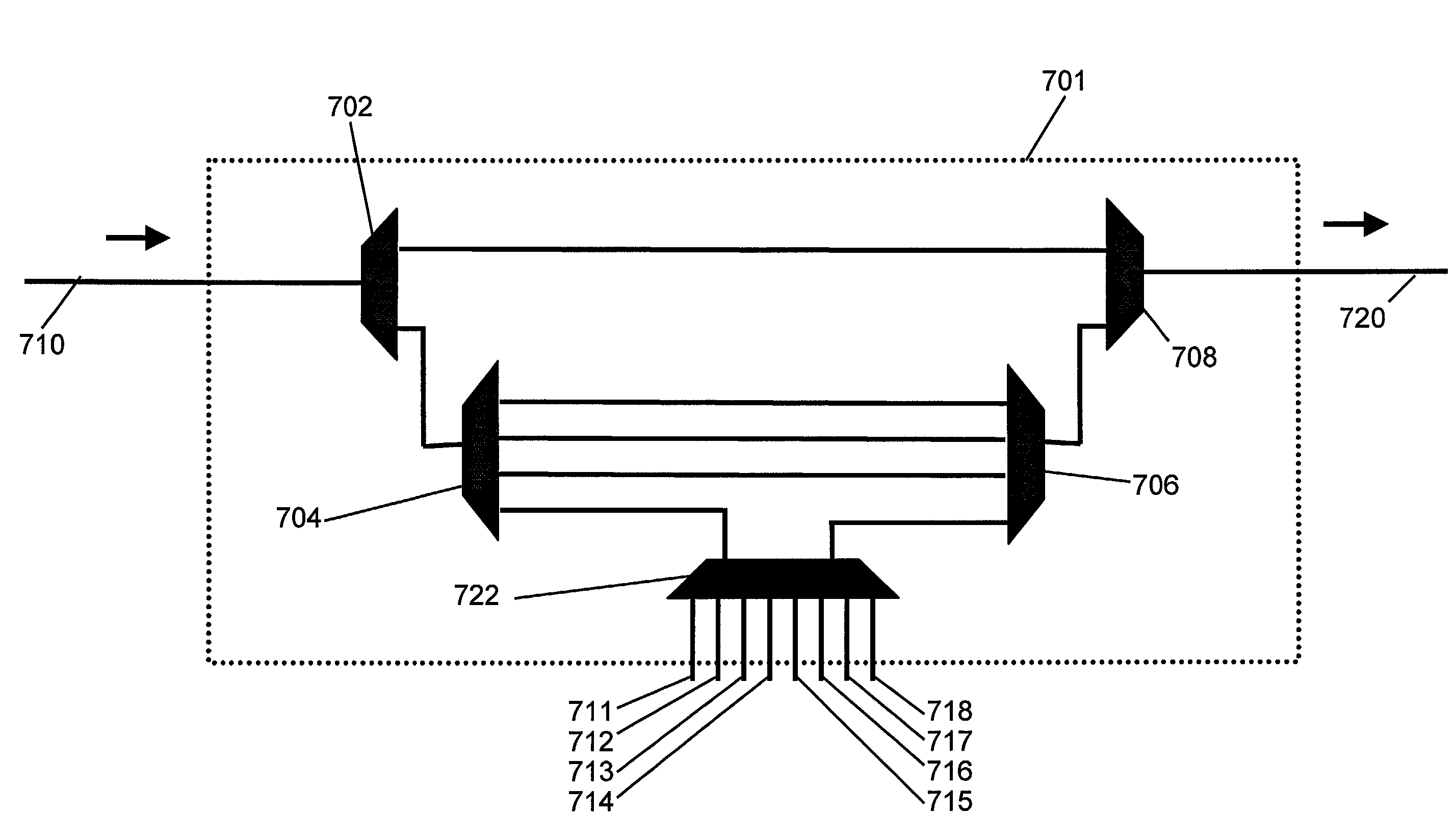
[0057] Referring to FIGS. 7-9 there is shown the present invention. FIG. 7 shows a schematic diagram of an improved OADM device 701. The OADM contains two demultiplexors 702, 704, two multiplexors 706, 708, 5 input ports 710, 715-718, 5 output ports 711-714, 720 and an integrated add-drop channel filter 722.

[0058] An optical signal enters the OADM 701 along the optical input path 710. The optical signal carries 32 channels each on a different wavelength of light; channels 1-4, 6-9, 11-14, 16-19, 21-24, 26-29, 31-34 and 36-39. Every fifth channel is not used as this relaxes the wavelength accuracy and filter shape tolerances for the demultiplexors 702, 704 and multiplexors 706, 708 within the OADM. The demultiplexor 702 splits the input optical signal into two groups of wavelengths and outputs each along a different optical path. The first group of wavelengths (channels 1-4, 6-9, 11-14 and 16-19) is then input to a second demultiplexor 704, also called a band drop filter. This demult...

second embodiment

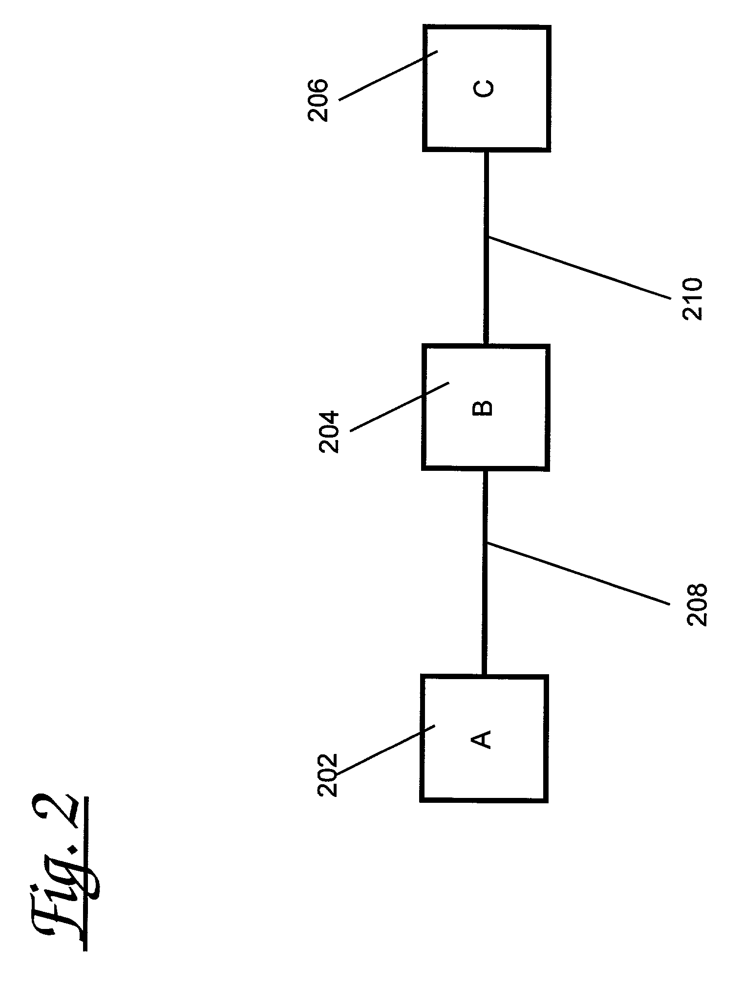
[0069] Referring to FIGS. 9-12 there is shown the present invention. A schematic diagram of an optical communications network is shown in FIG. 9. The network shown in FIG. 9 connects 6 different locations, A to F. It comprises 5 optical paths 902, 906, 910, 914, 918 and 4 OADMs 904, 908, 912, 916. An optical signal sent from location A travels along optical path 902. At location B there is an OADM 904 which drops and adds channels 1-4. The signal continues along optical path 906 until it reaches location C, where an OADM 908 drops and adds channels 6-9. The signal then continues along optical path 910 until it reaches location D, where an OADM 912 drops and adds channels 11-14. The signal then continues along optical path 914 until it reaches location E, where an OADM 916 drops and adds channels 16-19. The signal then continues to location F along optical path 918.

[0070] In addition to cost, size and power consumption, another important parameter when designing an optical system, ne...


PUM


Abstract

The invention is directed to an optical grating device which is capable of processing at least two optical signals concurrently, comprising a plurality of input waveguides, a plurality of output waveguides, a first free propagating region and a second free propagating region, and a composite light pathway. These are arranged such that a first input waveguide and a first output waveguide are connected to said first region; a second input waveguide and a second output waveguide are connected to said second region; and said first region and said second region are connected by the composite light pathway. Light input along the first input waveguide is able to pass through the composite light pathway to be output through the second output waveguide and light input along the second input waveguide is able to pass through the composite light pathway to be output through the first output waveguide. An advantage of such an optical grating device is that it combines the function of two optical grating devices into a single device, this leads to many advantages including reducing size, cost and power consumption.

Description

[0001] The present invention relates to an optical grating device.BACKGROUND TO THE INVENTION[0002] An optical communications system comprises a light source, such as a laser, a medium through which the light is transmitted, such as an optical fibre and a means of detecting the light, such as a photodetector. The component containing the light source is known as the transmitter and the component containing the detecting means is known as the receiver. The purpose of a communications system is to transfer information from one location to another. The output from the light source is modulated to encode this information and the modulation is detected by the receiver such that data is transmitted through the system.[0003] The term "light" with reference to an optical communications system is used herein to refer to electromagnetic radiation from any part of the electromagnetic spectrum.[0004] As the requirement to transfer data across an optical communication system increases, there are...

Claims


Application Information

Patent Timeline
IPC IPC(8): G02B6/34H04J14/02
CPCH04J14/0209G02B6/12021
Inventor KIRKBY, PAUL A.WHITEAWAY, JAMES E.
Owner BOOKHAM TECH
Why Eureka
Try Eureka