Crosslink cyclo-siloxane compound with linear bridging group to form ultra low k dielectric

a technology of cyclosiloxane and linear bridging group, which is applied in the direction of liquid surface applicators, coatings, chemical vapor deposition coatings, etc., can solve the problem of difficult to achieve product consistency

Inactive Publication Date: 2003-10-16
APPLIED MATERIALS INC
View PDF82 Cites 65 Cited by
  • Summary
  • Abstract
  • Description
  • Claims
  • Application Information

AI Technical Summary

Problems solved by technology

However, this method of partially fragmenting cyclic precursors is diff

Method used


Image

  • Crosslink cyclo-siloxane compound with linear bridging group to form ultra low k dielectric
  • Crosslink cyclo-siloxane compound with linear bridging group to form ultra low k dielectric
  • Crosslink cyclo-siloxane compound with linear bridging group to form ultra low k dielectric

Examples


example 1

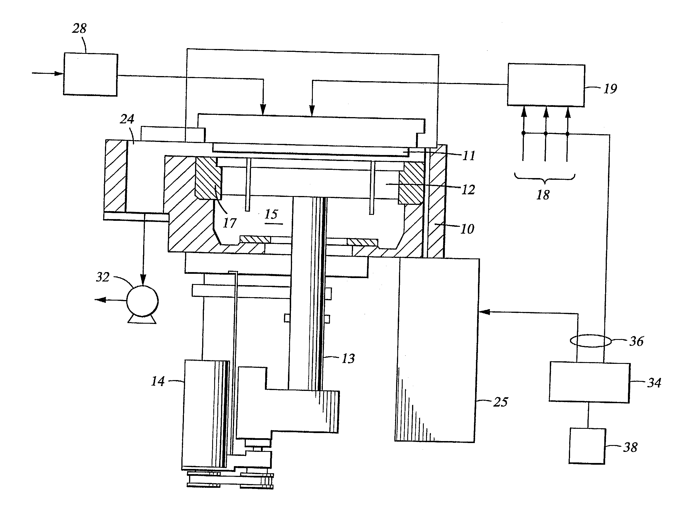
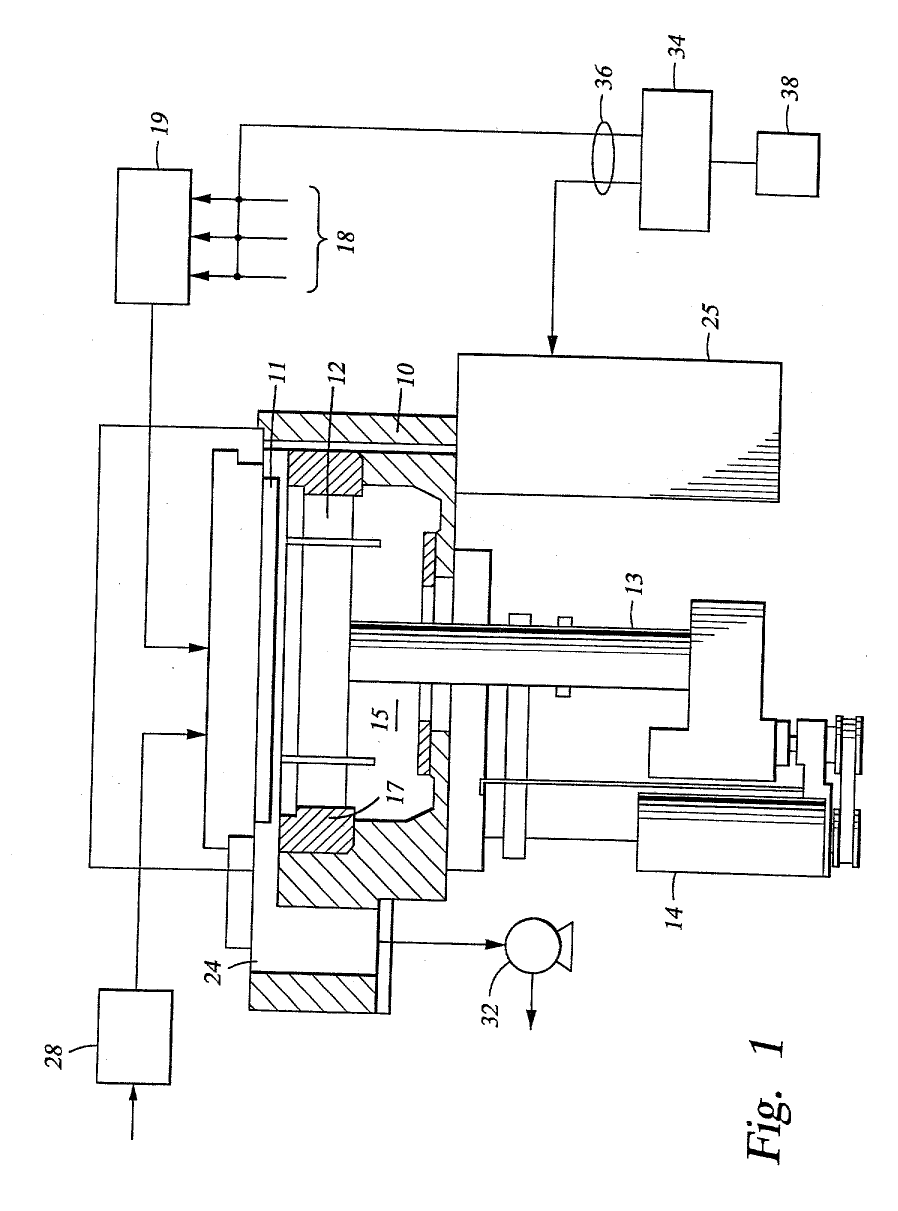
[0084] A low dielectric constant film was deposited on a 200 mm substrate from the following reactive gases at a chamber pressure of about 6 Torr and substrate temperature of about 400.degree. C.

[0085] Octamethylcyclotetrasiloxane (OMCTS), at about 520 sccm;

[0086] Trimethylsilane (TMS), at about 200 sccm;

[0087] Ethylene, at about 2,000 sccm;

[0088] Oxygen, at about 1,000 sccm; and

[0089] Helium, at about 1,000 sccm

[0090] The substrate was positioned 1,050 mils from the gas distribution showerhead. A power level of about 800 W at a frequency of 13.56 MHz was applied to the showerhead for plasma enhanced deposition of the film. The film was deposited at a rate of about 12,000 A / min, and had a dielectric constant (k) of about 2.54 measured at 0.1 MHz.

example 2

[0091] A low dielectric constant film was deposited on a 200 mm substrate from the following reactive gases at a chamber pressure of about 6 Torr and substrate temperature of about 400.degree. C.

[0092] Octamethylcyclotetrasiloxane (OMCTS), at about 520 sccm;

[0093] Trimethylsilane (TMS), at about 400 sccm;

[0094] Ethylene, at about 2,000 sccm;

[0095] Oxygen, at about 1,000 sccm; and

[0096] Helium, at about 1,000 sccm;

[0097] The substrate was positioned 1,050 mils from the gas distribution showerhead. A power level of about 800 W at a frequency of 13.56 MHz was applied to the showerhead for plasma enhanced deposition of the film. The film was deposited at a rate of about 12,000 A / min, and had a dielectric constant (k) of about 2.51 measured at 0.1 MHz.

example 3

[0098] A low dielectric constant film was deposited on a 200 mm substrate from the following reactive gases at a chamber pressure of about 6 Torr and substrate temperature of about 400.degree. C.

[0099] Octamethylcyclotetrasiloxane (OMCTS), at about 520 sccm;

[0100] Trimethylsilane (TMS), at about 600 sccm;

[0101] Ethylene, at about 2,000 sccm;

[0102] Oxygen, at about 1,000 sccm; and

[0103] Helium, at about 1,000 sccm

[0104] The substrate was positioned 1,050 mils from the gas distribution showerhead. A power level of about 800 W at a frequency of 13.56 MHz was applied to the showerhead for plasma enhanced deposition of the film. The film was deposited at a rate of about 12,000 A / min, and had a dielectric constant (k) of about 2.47 measured at 0.1 MHz.


PUM

PropertyMeasurementUnit
Timeaaaaaaaaaa
Pressureaaaaaaaaaa
Pressureaaaaaaaaaa

Abstract

A method for depositing a low dielectric constant film having a dielectric constant of about 3.0 or less, preferably about 2.5 or less, is provided by using one or more cyclic organic precursors and one or more aliphatic precursors. In one aspect, a cyclic organosilicon compound, an aliphatic organosilicon, and an aliphatic hydrocarbon compound are reacted with an oxidizing gas at conditions sufficient to deposit a low dielectric constant film on the semiconductor substrate. The cyclic organosilicon compound includes at least one silicon-carbon bond. The aliphatic organosilicon compound includes a silicon-hydrogen bond or a silicon-oxygen bond.

Description

BACKGROUND OF THE DISCLOSURE[0001] 1. Field of the Invention[0002] Embodiments of the present invention relate to the fabrication of integrated circuits. More particularly, embodiments of the present invention relate to a process for depositing dielectric layers on a substrate.[0003] 2. Background of the Invention[0004] Integrated circuit geometries have dramatically decreased in size since such devices were first introduced several decades ago. Since then, integrated circuits have generally followed the two year / half-size rule (often called Moore's Law), which means that the number of devices on a chip doubles every two years. Today's fabrication facilities are routinely producing devices having 0.13 .mu.m and even 0.1 .mu.m feature sizes, and tomorrow's facilities soon will be producing devices having even smaller feature sizes.[0005] The continued reduction in device geometries has generated a demand for films having lower k values because the capacitive coupling between adjacent...

Claims


Application Information

Patent Timeline
IPC IPC(8): C09D4/00C23C16/40H01L21/312
CPCC09D4/00C23C16/401H01L21/02126H01L21/02211H01L21/02216H01L21/3122H01L21/02274C08G77/00
Inventor LI, LIHUAZHU, WEN H.HUANG, TZU-FANGXIA, LI QUNYIEH, ELLIE
Owner APPLIED MATERIALS INC
Why Eureka
Try Eureka