Semiconductor device having improved insulation film and manufacturing method thereof

a technology of insulation film and semiconductor, applied in the direction of semiconductor device, semiconductor/solid-state device details, electrical apparatus, etc., can solve the problems of deteriorating the resistance of the film to moisture absorption, line delay, and film density reduction

Inactive Publication Date: 2000-03-07
MITSUBISHI ELECTRIC CORP
View PDF7 Cites 27 Cited by
  • Summary
  • Abstract
  • Description
  • Claims
  • Application Information

AI Technical Summary

Problems solved by technology

The recent finer patterning of semiconductor devices has posed a serious problem with lead line delay due to the capacitance of the interlayer insulating film.
And such minute voids lead to a decrease in film density.
These minute voids (defects) present a new problem of deteriorating the resistance of the film to moisture absorption.
The result is that the film changes into one which contains a large amount of moisture.

Method used


Image

  • Semiconductor device having improved insulation film and manufacturing method thereof
  • Semiconductor device having improved insulation film and manufacturing method thereof
  • Semiconductor device having improved insulation film and manufacturing method thereof

Examples


Embodiment Construction

Preferred embodiments of the invention will now be described with reference to the accompanying drawings in which like reference characters designate like or corresponding parts.

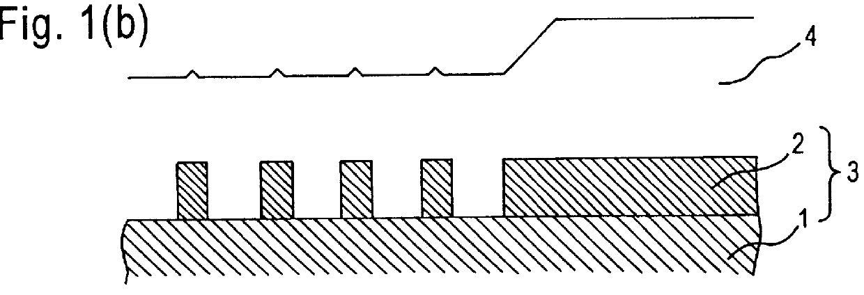
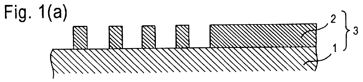
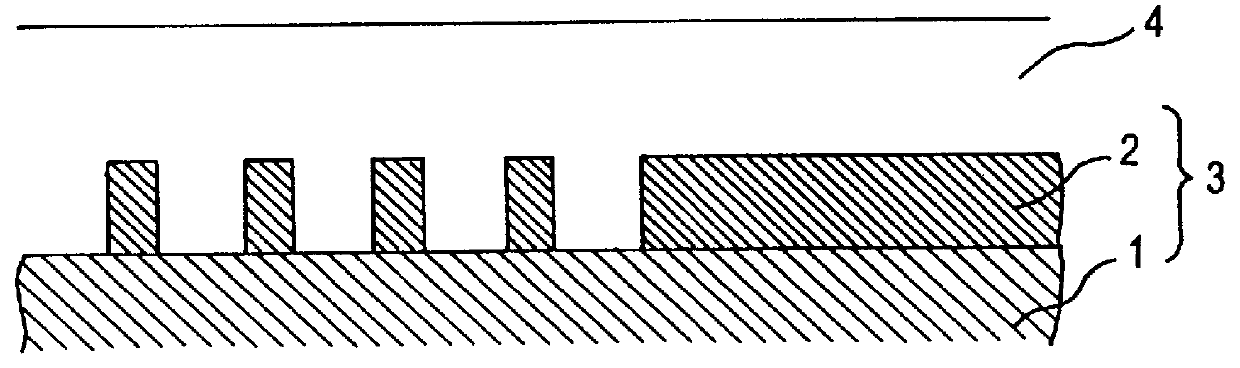
FIG. 1 shows a process for forming an interlayer insulating film according to one embodiment of the present invention.

The process starts with preparing a silicon substrate 1 on which are formed elements and insulating layers (not shown), as shown in FIG. 1(a). On this substrate 1 is formed an aluminum interconnection 2 of a desired pattern. In this way a wafer 3 is obtained in the first step.

In the second step, the wafer 3 is covered with an interlayer insulating film 4 of SiOF by the high-density plasma chemical vapor deposition method (CVD), as shown in FIG. 1(b). A detailed description of this method is given later.

In the third step, the SiOF film 4 formed by the high-density plasma CVD method is made flat by the chemical mechanical polishing method (CMP), as shown in FIG. 1(c).

This step is usually follow...


PUM


Abstract

A semiconductor device which has an interlayer insulating film comprised of molecules with silicon-oxygen bonds and silicon-fluorine bonds and contains a rare gas in concentration higher than 1011 atoms per cm2. The interlayer insulating film is preferably a fluorine-containing silicon oxide film which contains a rare gas. In a manufacturing process, an interlayer insulating is formed by a chemical vapor deposition from a material gas including a silicon-containing gas, a fluorine compound gas, a rare gas, and oxygen. The silicon-containing gas is preferably SiH4 gas, and the fluorine compound gas is preferably SiF4 gas. The flow rate of the rare gas is greater than three times the total flow rate of the SiH4 gas and SiF4 gas. The rare gas is at least one type of gas selected from neon (Ne), argon (Ar), krypton (Kr), and xenon (Xe).

Description

1. Field of the InventionThe present invention relates to a semiconductor device and a process for manufacturing the same. More particularly, the present invention relates to a semiconductor device having an improved interlayer insulating film and a process for manufacturing the same.2. Background ArtThe recent finer patterning of semiconductor devices has posed a serious problem with lead line delay due to the capacitance of the interlayer insulating film. Reducing the capacitance of the interlayer insulating film is an important future subject. This is true particularly in the case of lead lines finer than 0.3 m. Thus, there is a demand for a new interlayer insulating film which has a low dielectric constant and good burying properties and surface leveling properties.It is expected that this demand will be satisfied by fluorine-containing silicon oxide film (referred to as SiOF film hereinafter). See "High density plasma CVD fluoro-silicate glass gap-filling for sub-half micron CM...

Claims


Application Information

Patent Timeline
Patent Type & Authority Patents(United States)
IPC IPC(8): H01L23/52H01L23/532H01L21/768H01L21/316H01L23/522
CPCH01L23/5329H01L2924/0002H01L2924/00H01L21/31
Inventor MATSUURA, MASAZUMI
Owner MITSUBISHI ELECTRIC CORP
Why Eureka
Try Eureka