Image sensor, method of fabricating the same, and exposure apparatus, measuring device, alignment device, and aberration measuring device using the image sensor

a technology of image sensor and manufacturing method, which is applied in the field of backilluminated image sensor, can solve the problems of low efficiency of energy ray detection, difficult to improve the resolution of image sensor, and complicating the peripheral mechanism of image sensor

Inactive Publication Date: 2004-01-15
NIKON CORP
View PDF9 Cites 65 Cited by
  • Summary
  • Abstract
  • Description
  • Claims
  • Application Information

AI Technical Summary

Benefits of technology

[0025] Another object of the present invention is to provide a back-illuminated image sensor capable of suppressing dark current from the second-plane side.
[0026] Another object of the present invention is to provide a back-illuminated image sensor capable of suppressing dark current from the first-plane side.
[0027] Another object of the present invention is to provide a back-illuminated image sensor in which it is possible to reliably transfer a charge in a charge accumulating unit to a charge transfer unit.

Problems solved by technology

Accordingly, there has been a problem that the electrons tend to recombine with holes and disappear, with a low efficiency of energy ray detection.
There has been another problem that the electrons traveling through the semiconductor base 602 get mixed between pixels, and thereby cause smear.
On that account, the smear production makes it extremely difficult to improve the image sensor in resolution.
Therefore, in the cases of short-wavelength energy rays, the above-mentioned two problems tend to be more significant since electrons have particularly longer traveling distances.
Meanwhile, there has been another problem that the characteristics of the image sensor 601 largely depend on the impurity concentration and thickness of the semiconductor base 602.
Thus, there has been a problem that the conventional image sensor 601 requires a mechanical shutter, which complicates the peripheral mechanisms of the image sensor.
Such dark current have caused unwanted effects including a deterioration in imaging quality and the impossibility of weak light detection.
The backside wells capture electrons and lower the efficiency of the energy ray detection.
Double side aligners, however, produce alignment errors of .+-.2 .mu.m.
Thus, it has been extremely difficult in principle to improve the precision of the alignment.
Accordingly, there has been a problem that whichever aligner is used, double-sided structure cannot be aligned with precision.
The results in less possibilities of causing image lag phenomena due to signal charges left in the charge accumulating units.
In this case, the lower impurity concentration rate of the semiconductor base significantly reduces such production defects as "uneven transportation of signal charges" and "the production of defective pixels" because of unevenness and variations in the fabrication conditions of the semiconductor base.

Method used


Image

  • Image sensor, method of fabricating the same, and exposure apparatus, measuring device, alignment device, and aberration measuring device using the image sensor
  • Image sensor, method of fabricating the same, and exposure apparatus, measuring device, alignment device, and aberration measuring device using the image sensor
  • Image sensor, method of fabricating the same, and exposure apparatus, measuring device, alignment device, and aberration measuring device using the image sensor

Examples


first embodiment

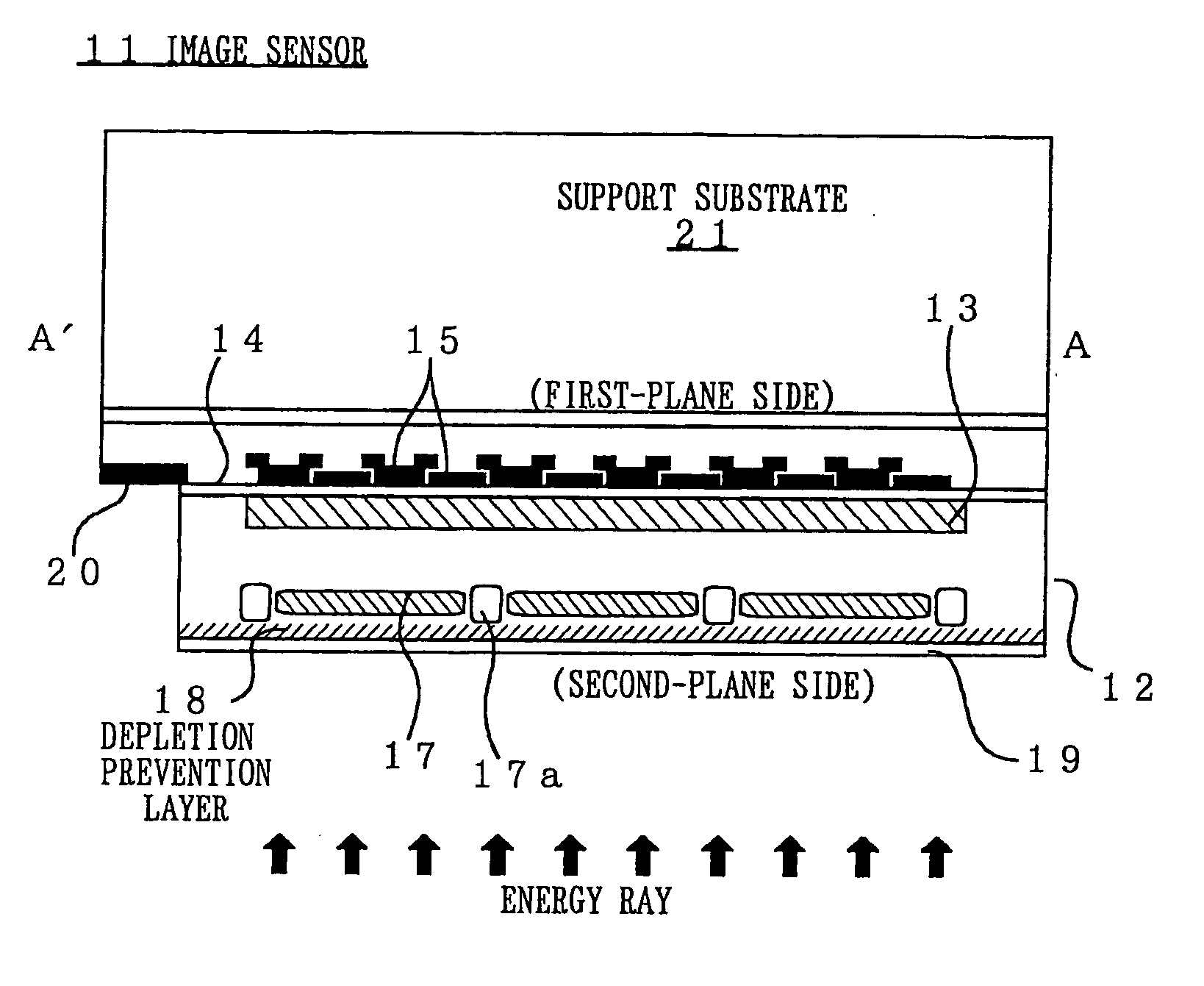
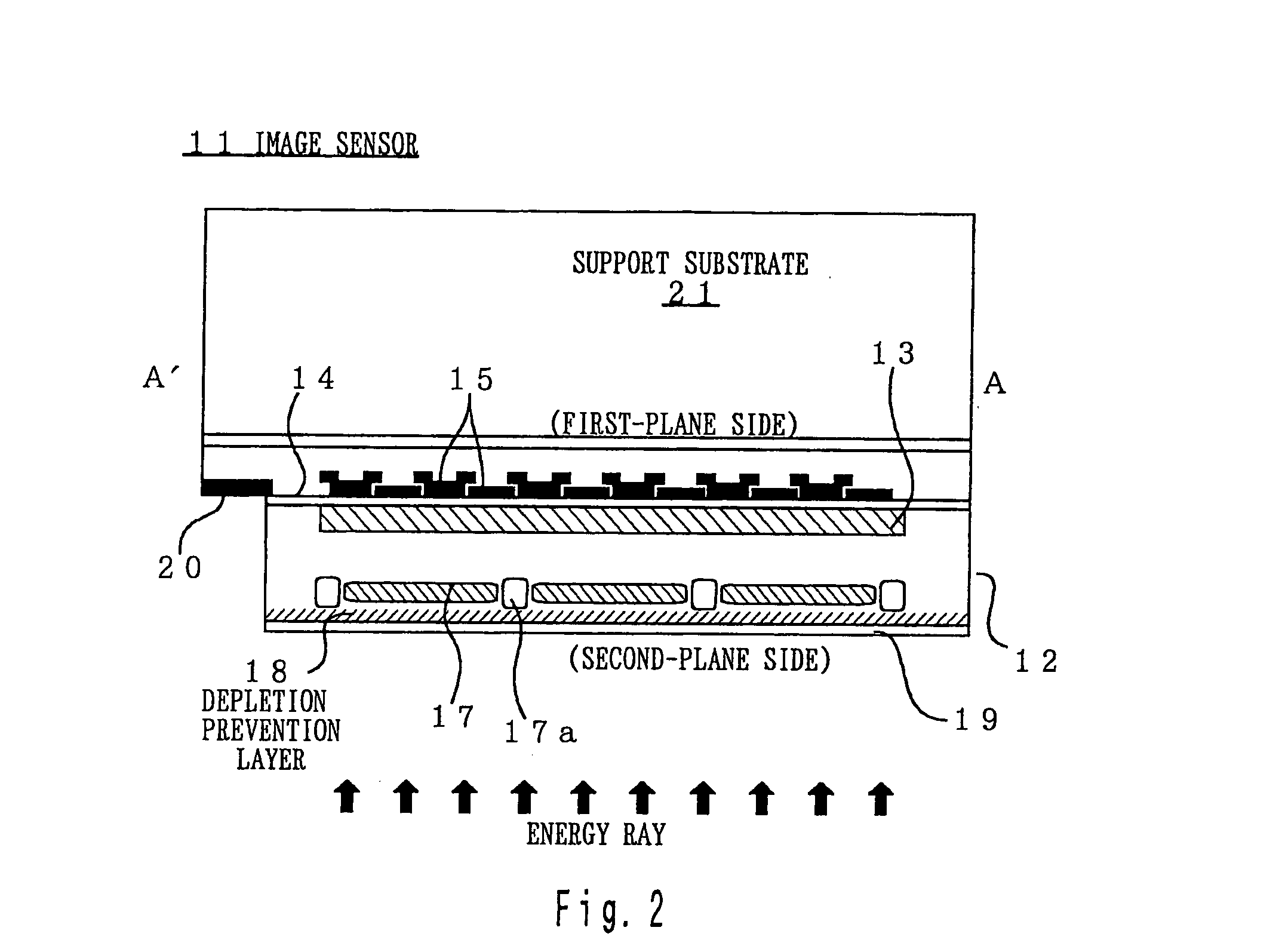
[0222] In the first embodiment described above, the charge accumulating units 17 are arranged on the second-plane side, opposite to the CCD diffusion layers 13. This allows a substantial reduction in the traveling distances of the signal charges on the second-plane side. As a result, it becomes possible to improve the efficiency of energy ray detection and the production of smear. In particular, the above-mentioned improvements become more significant when the traveling distances are longer (when signal charges are generated at very shallow depth in the second plane as under ultraviolet rays).

[0223] Besides, in the first embodiment, the dark current are suppressed greatly owing to a synergistic effect of the depletion prevention layer 18, the discharging of the dark current, the prevented surface depletion of the CCD diffusion layers 13, and so on. Accordingly, it becomes possible to obtain relatively favorable imaging quality even under severe conditions such as weak light detectio...

second embodiment

[0231] The second embodiment corresponds to the inventions set forth in claims 1-10.

[0232] FIG. 11 is a sectional view of an image sensor 51 according to the second embodiment. Note that configurations common to those of the first embodiment (FIG. 2) are shown in FIG. 11 with identical numerals attached thereto. Description thereof will be omitted here.

[0233] A constitutional feature of the image sensor 51 lies in that the semiconductor base 12 is surrounded by an N-type region 52 (corresponding to the semiconductor region described in claim 9) so that the semiconductor base 12 has a well structure. Incidentally, the well structure may be fabricated by forming an N.sup.+-type impurity region in the semiconductor base 12 as an isolation. Otherwise, it may be fabricated by forming a well-shaped P-type semiconductor 12 in part of an N-type semiconductor.

[0234] FIG. 12 is a potential chart for explaining the operation of the second embodiment.

[0235] In the second embodiment, as shown in...

third embodiment

[0240] The third embodiment is of the image sensors corresponding to the inventions set forth in claims 1-4 and 11-18.

[0241] [Configuration of the Image Sensor]

[0242] FIG. 13 is a diagram showing an image sensor 511 according to the third embodiment. FIG. 14 is a diagram showing the sectional structure along the B-B' part shown in FIG. 13. FIG. 15 is a chart showing the net impurity concentration in the A-A' part shown in FIG. 14.

[0243] A constitutional feature of the third embodiment lies in that as shown in FIGS. 13 and 14, a barrier region 519 is arranged between the charge accumulating units 17 and the CCD diffusion layers 13 so as to intercept the charge transporting paths. The barrier region 519 has an impurity concentration distribution of P-type as shown in FIG. 15. The semiconductor base 12 is previously set to be lower than the barrier region 519 in P-type impurity concentration rate.

[0244] Note that components common to those of the first embodiment (FIGS. 1 and 2) are sh...


PUM


Abstract

In the present invention, a charge transfer unit is arranged on a first-plane side of a thinly-formed semiconductor base. Charge accumulating units are arranged on a second-plane side, the opposite side. A depletion prevention layer is arranged closer to the second-plane side than the charge accumulating units. The depletion prevention layer prevents a depletion region around the charge accumulating units from reaching the second plane of the semiconductor base. The depletion prevention layer can suppress surface dark current going into the charge accumulating units. Meanwhile, an energy ray incident from the second-plane side pass through the depletion prevention layer to generate signal charges in the charge accumulating units (depletion regions). The charge accumulating units collect, on a pixel-by-pixel basis, the signal charges which are to be transported to the charge transfer unit under voltage control or the like, and then are read to exterior as image signals.

Description

[0001] This application is a continuation of U.S. application Ser. No. 09 / 908,181 filed Jul. 18, 2001, of the same title, and which is abandoned upon filing of the present application, which application Ser. No. 09 / 908,181 was a contination-in-part of pending U.S. patent application Ser. No. 09 / 810,227, filed Mar. 16, 2001.[0002] 1. Field of the Invention[0003] The present invention relates to a back-illuminated image sensor wherein energy rays (visible light, ultraviolet rays, soft X-rays, electron beams, and so on) are received at one plane side of a semiconductor (second-plane side) and optoelectronically converted signal charges are transported to a charge transfer unit on the other plane side (first-plane side) for readout.[0004] The present invention relates to a method of fabricating the image sensor.[0005] The present invention relates to a method of fabricating a device such as the image sensor where alignment of its double-sided structure is required.[0006] The present inv...

Claims


Application Information

Patent Timeline
Patent Type & Authority Applications(United States)
IPC IPC(8): H01L27/146H01L27/148H01L29/768
CPCH01L27/1463H01L27/14643H01L27/14654H01L27/1464H01L27/14687H01L27/14689H01L27/14806H01L27/14683
Inventor NARUI, TADASHIAKAGAWA, KEIICHIYAGI, TAKESHI
Owner NIKON CORP
Why Eureka
Try Eureka