System and method for correcting timing signals in integrated circuits
a timing signal and integrated circuit technology, applied in the field of timing system for integrated circuits, can solve problems such as existing margins
- Summary
- Abstract
- Description
- Claims
- Application Information
AI Technical Summary
Benefits of technology
Problems solved by technology
Method used
Image
Examples
first embodiment
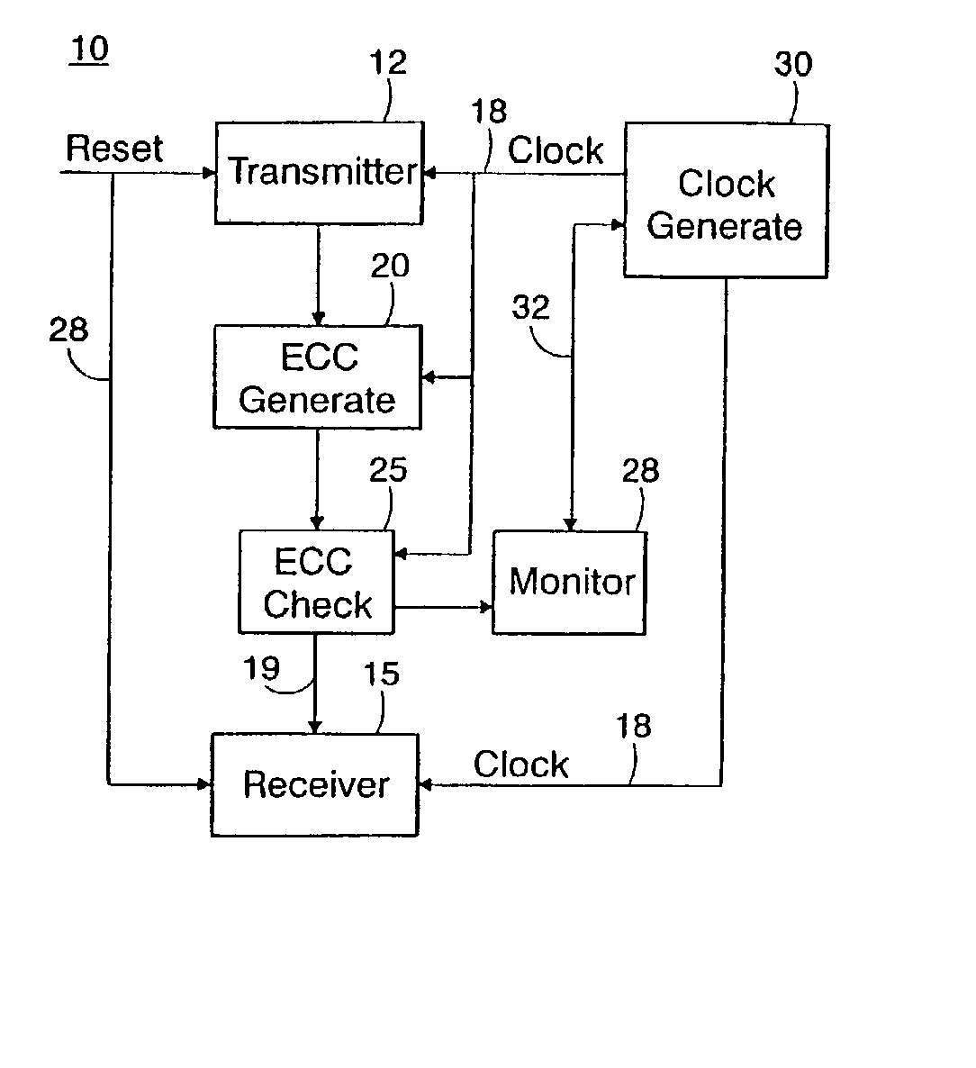
[0020] FIG. 1 is a block diagram depicting the novel error correcting system architecture 10 according to the invention. As shown in FIG. 1, there is provided a source circuit device 12 for transmitting data signals through ECC error correction circuitry 20 to a destination device such as IC receiver device 15 according to clock timing signals 18 provided by clock generator circuit 30. As shown in FIG. 1, the source transmitter circuit 12 is coupled to an error correcting code (ECC) generator circuit device 20 that generates ECC bits in accordance with the data that is received from the transmitter 12. The ECC generator 20 receives data from the transmitter 12 and, outputs the data plus error correction information according to known techniques. Coupled to the ECC generator device 20 is a novel error correcting code (ECC) check circuit device 25 which, in turn, is coupled to a destination receiver device 15 for receiving the transmitted data. As will be described in further detail h...
second embodiment
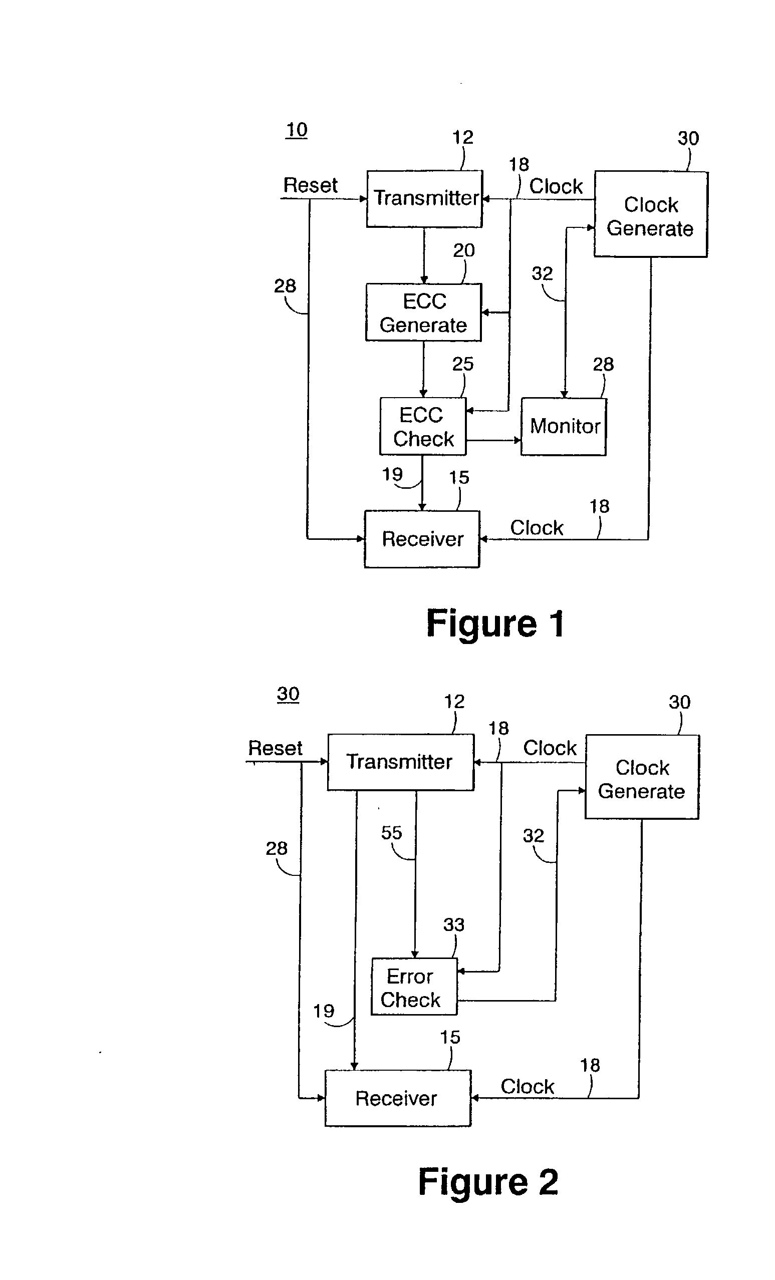
[0023] Preferably, at reset, a learning cycle is implemented where a series of predefined transmissions is generated from the transmit source 12. According to the invention, during the test time, the error check circuitry 33 (FIG. 2) will monitor to a first fail point, and then pick a clock tap of sufficient guard band to guarantee the error free arrival of the data. That is, as the error check circuit 30 is informed of the bit signal patterns output from the transmitter, it knows what signals to expect at each iteration. Thus, during the learning cycle, for each one or a series of outputs generated from the transmit source 12, the clock signal 18 is gradually increased, for example. Thus, the generated signal patterns along line 55 are sufficiently delayed so that they may be read by the error checker circuit 33. As the clock signal 18 input to the transmitter effects the timing of signals generated at the transmit source 12, the error check circuit will monitor the delayed transm...
third embodiment
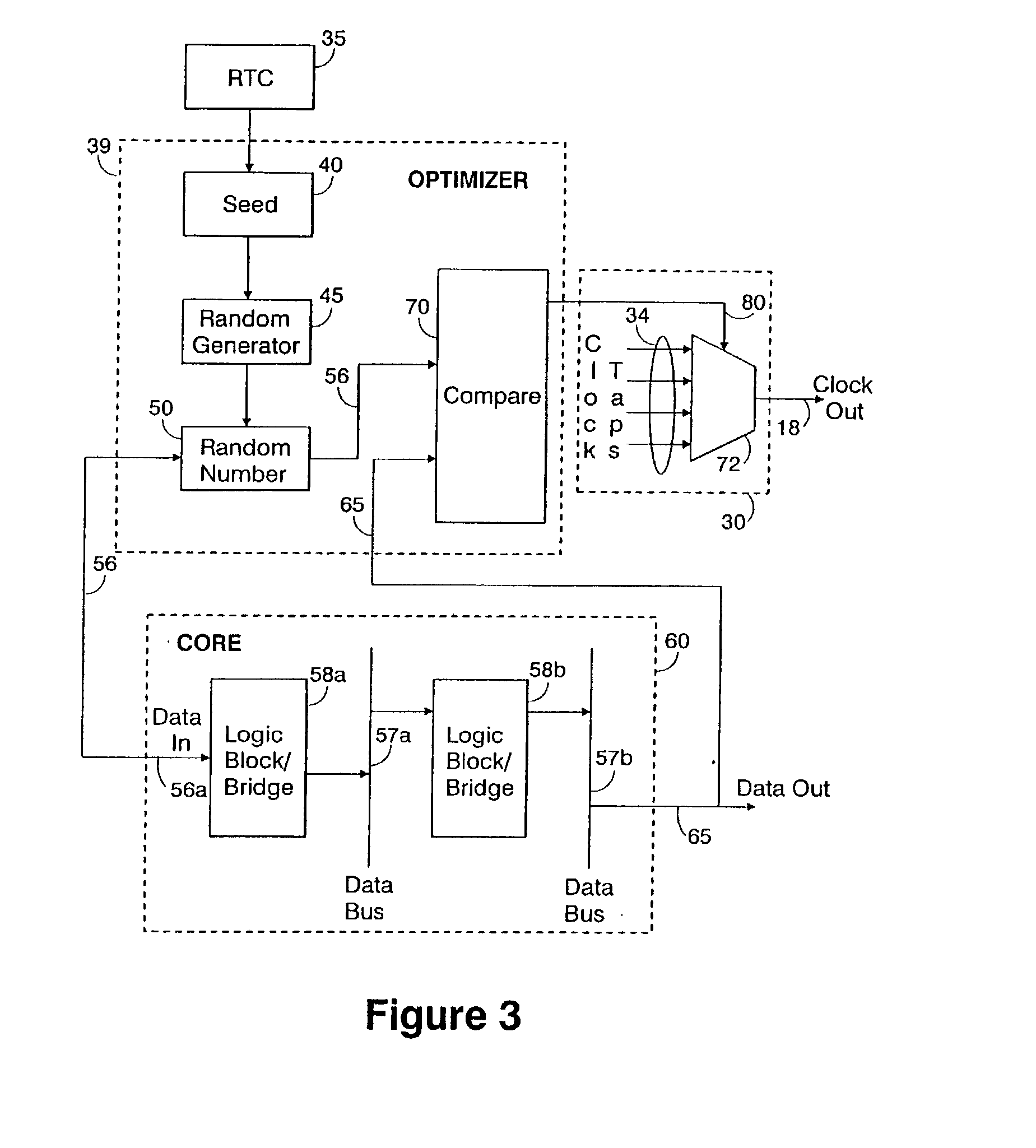
[0027] shown in FIG. 3, there is depicted a detailed dataflow diagram of the error generation and correction circuitry 75. In this embodiment, at system reset, the current value of the Real Time Clock (RTC) 35 is input to an optimizer circuit 39 comprising a SEED register 40 which seeds a random number generator 45. In one embodiment, a SEED is initialized, and then incremented every clock cycle. With this SEED, a unique random number 56 is generated with any pseudo-random, linearly distributed algorithm known to skilled artisans (such as XORing the bits with themselves). This unique random number 56 is transmitted throughout a data path of a semiconductor circuit, e.g., a "system on chip", also referred to as a CORE circuit 60 comprising the IC, in FIG. 3.
[0028] Particularly, this random data 56 is fed to the start of the dataflow path 56a at the input of the CORE circuit 60 and the data is transmitted through various asynchronous busses or serial data streams. In one embodiment d...
PUM
 Abstract
Description
Claims
Application Information


