Organic thin film transistor and method of manufacturing the same, and semiconductor device having the organic thin film transistor

a thin film transistor and organic technology, applied in semiconductor devices, solid-state devices, electrical equipment, etc., can solve the problems of not being able to apply the method, not being able to meet the requirements of large-scale use of effective substrate materials, and requiring a lot of material and man-hours for maintenance of apparatuses

Inactive Publication Date: 2004-02-05
SEMICON ENERGY LAB CO LTD
View PDF17 Cites 116 Cited by
  • Summary
  • Abstract
  • Description
  • Claims
  • Application Information

AI Technical Summary

Benefits of technology

[0011] Further, another object of the present invention is to provide a method of manufacturing an organic semiconductor film, in which a thin and uniform organic semiconductor film can be formed.
[0016] According to the present invention as described above, the semiconductor film with a very thin thickness (approximately several tens to 100 .ANG.) can be formed. Further, according to the present invention, the organic semiconductor film can be formed with efficiency, and thus, there is an expectation for simplification of the manufacturing process.
[0017] Further, according to the present invention, the organic semiconductor film can be formed only at the specific spot. Thus, apparatus maintenance and cost of cleaning solution and material can be eliminated, and therefore, total cost can be reduced. As a result, a low-cost semiconductor device provided with an organic TFT can be provided. Further, according to the present invention, there can be provided a method of manufacturing an organic semiconductor film, with which materials to be wasted and discarded are eliminated, with which liquid wastes along with apparatus maintenance and cleaning are not produced, and which is friendly to the environment.

Problems solved by technology

However, there is a problem that lots of effective substrate materials can't be used since its processing temperature is above 350.degree. C. when TFTs are manufactured using inorganic semiconductor materials.
However, there have been problems that any of the above manufacturing methods requires a special apparatus, and that formed organic semiconductor films are so little to quantity consumed materials and most of the used materials are discarded in the end.
Therefore, a great cost for materials and man-hours for maintenance of apparatus have been required.
As a result, it has not been desirable to apply these methods not only for the effect on the production cost, but also the disastrous effect on the environment generated from material wastes and liquid wastes.
It is difficult to coat the films separately by spin coating, so that patterning is required after coating the organic films allover.
It is still difficult to perform patterning with absolute precision by this method.
In addition, ink jetting, printing and some other ways have not yet come into practical use.
Moreover, in the methods above, it is difficult to form a thin and uniform organic semiconductor film and to attain a TFIF characteristic.

Method used


Image

  • Organic thin film transistor and method of manufacturing the same, and semiconductor device having the organic thin film transistor
  • Organic thin film transistor and method of manufacturing the same, and semiconductor device having the organic thin film transistor
  • Organic thin film transistor and method of manufacturing the same, and semiconductor device having the organic thin film transistor

Examples


embodiment 1

[0125] [Embodiment 1]

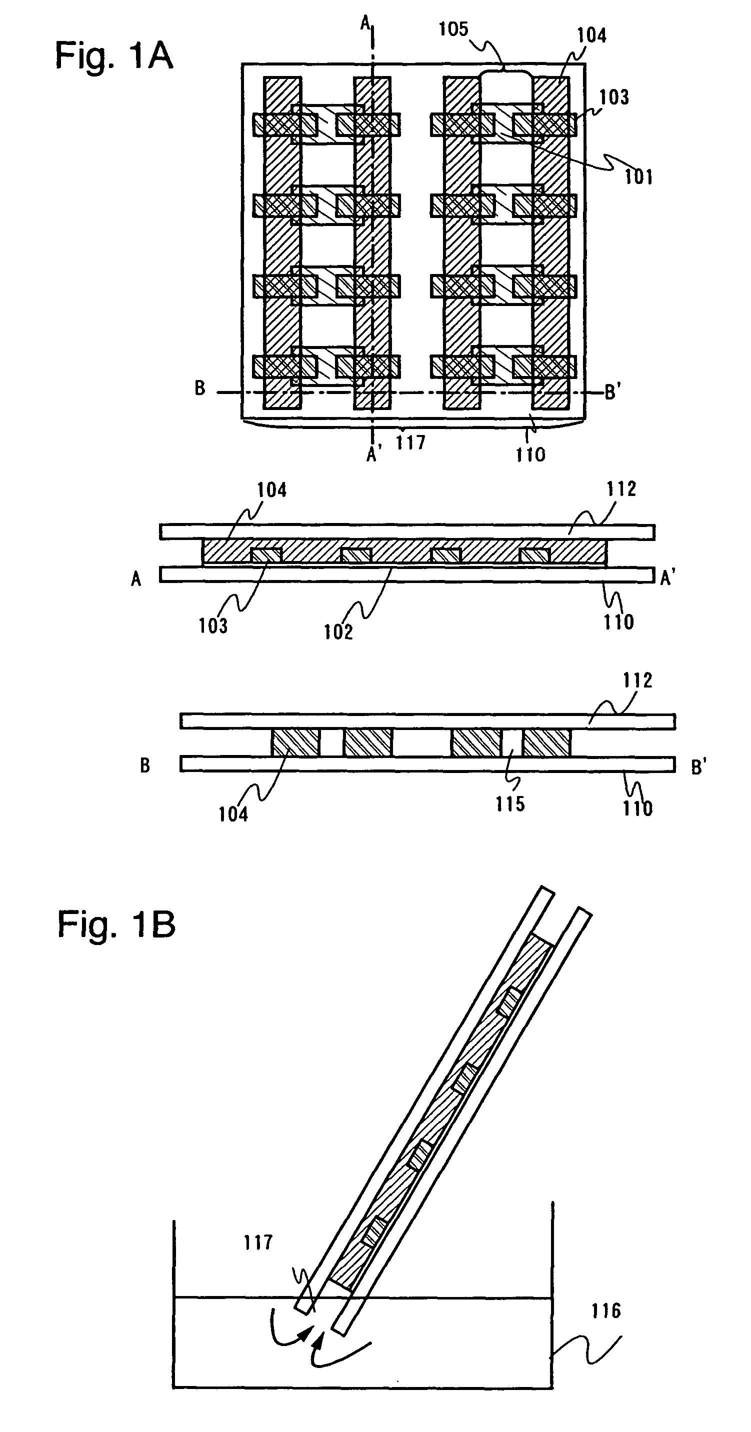
[0126] In this embodiment, Vd-Id characteristics and VG-Id characteristics were measured with the use of the organic TFT of the present invention. Note that, as shown in FIG. 10, the organic TFT as a measurement sample has a structure in which, in an atmosphere: a gate electrode 1003 formed of tungsten is provided on a quartz substrate; a gate insulating film is provided on the gate electrode; a source electrode 1001 and a drain electrode 1002 which are formed of tungsten are provided on the gate insulating film so as to intersect each other in a comb form; and an organic semiconductor film is provided between the source electrode and the drain electrode. Then, the source electrode 1001, the drain electrode 1002, and the gate electrode 1003 are respectively provided with measurement pads (source electrode pad 1011, drain electrode pad 1012, and gate electrode pad 1013) for application of a measurement voltage and detection of a current.

[0127] Further, a channel ...


PUM

PropertyMeasurementUnit
thicknessaaaaaaaaaa
thicknessaaaaaaaaaa
pore sizeaaaaaaaaaa

Abstract

There have been problems in that a dedicated apparatus is needed for a conventional method of manufacturing an organic thin film transistor and in that: a little amount of an organic semiconductor film is formed with respect to a usage amount of a material; and most of the used material is discarded. Further, apparatus maintenance such as cleaning of the inside of an apparatus cup or chamber has needed to be frequently carried out in order to remove the contamination resulting from the material that is wastefully discarded. Therefore, a great cost for materials and man-hours for maintenance of apparatus have been required. In the present invention, a uniform organic semiconductor film is formed by forming an aperture between a first substrate for forming the organic semiconductor film and a second substrate used for injection with an insulating film formed at a specific spot and by injecting an organic semiconductor film material into the aperture due to capillarity to the aperture. The insulating film formed at the specific spot enables formation of the organic semiconductor film with high controllability. Further, the insulating film can also serve as a spacer that holds the aperture, that is, an interval (gap) between the substrates.

Description

[0001] 1. Field of the Invention[0002] The present invention relates to a thin film transistor having an organic semiconductor film and a manufacturing method thereof. In addition, the present invention relates to a semiconductor device provided with the above thin film transistor and a manufacturing method thereof.[0003] 2. Description of the Related Art[0004] A display device provided with thin film transistors (TFTs) has been studied recent years. The display device provided with TFTs can be operated in low-power consumption and occupy small space compared with CRT, therefore it has been used for a display portion of a personal computer, a PDA, or the like. These TFTs have been practically manufactured using inorganic semiconductor materials such as amorphous silicon, crystalline silicon, or the like. However, there is a problem that lots of effective substrate materials can't be used since its processing temperature is above 350.degree. C. when TFTs are manufactured using inorga...

Claims


Application Information

Patent Timeline
Patent Type & Authority Applications(United States)
IPC IPC(8): H01L21/00H01L21/77H01L21/84H01L27/12H01L51/00H01L51/30H01L51/40
CPCH01L51/0003H01L51/0545H01L51/0037H10K71/12H10K85/1135H10K10/466
Inventor HIRAKATA, YOSHIHARUISHITANI, TETSUJIFUKAI, SHUJIIMAHAYASHI, RYOTA
Owner SEMICON ENERGY LAB CO LTD
Why Eureka
Try Eureka