Flexible wiring boards

Inactive Publication Date: 2004-03-11
SONY CORP
View PDF28 Cites 2 Cited by
  • Summary
  • Abstract
  • Description
  • Claims
  • Application Information

AI Technical Summary

Benefits of technology

[0070] Fine metal bumps can be formed with good precision.[0071] A desired shape of opening (for example, square or hexagonal) can be formed because laser beam is not used.[0072] The selection of bump height of 35 .mu.m or less decreases variation in bump height to reduce failure of connection with non-flexible semiconductor chips such as IC chips.

Problems solved by technology

However, it becomes more difficult for the chemical solution to penetrate into openings 115, therefore it becomes more difficult to remove residues as openings 115 become finer.
Another problem is variation in the diameter of fine openings 115 (about 40 .mu.m to 50 .mu.m) formed by irradiating a rigid polyimide film 111 with laser beam 114, resulting in variation in the diameter and height of metal bumps 116 to cause failure of connection with semiconductor chips.
Still another problem is that it is difficult to reduce the spot diameter of high power laser beam 114, which makes it impossible to form openings 115 having a diameter smaller than 40 .mu.m contrary to the recent demand for further finer openings 115.

Method used


Image

  • Flexible wiring boards
  • Flexible wiring boards
  • Flexible wiring boards

Examples


Embodiment Construction

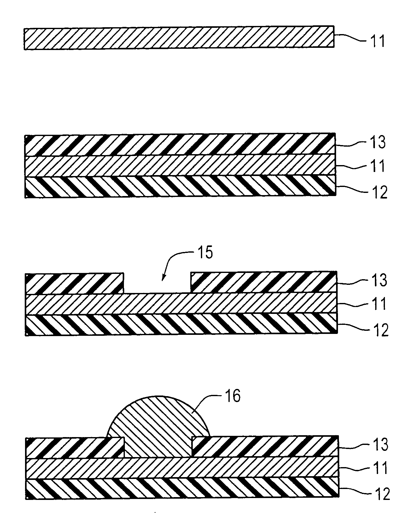
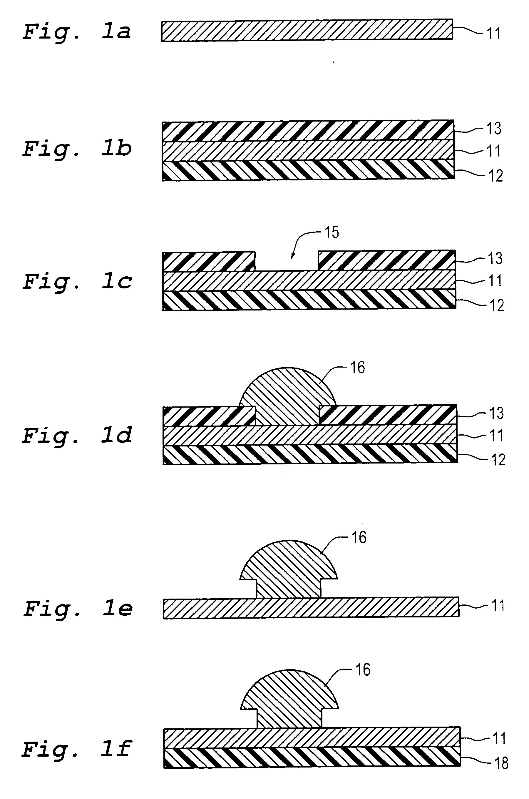
[0042] The present invention will now be described with reference to the attached drawings.

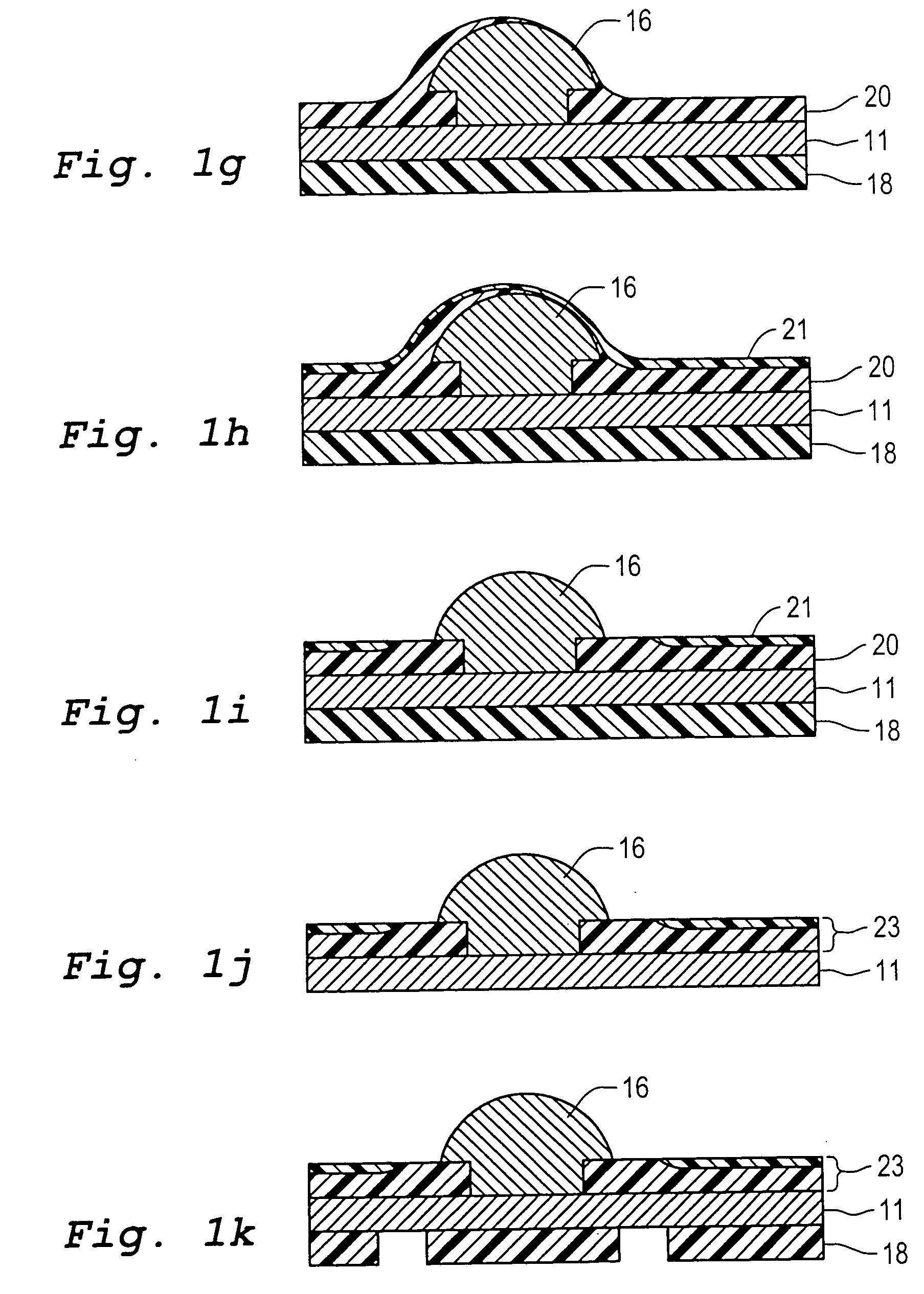
[0043] FIG. 1(a) to FIG. 1(p) is a processing diagram illustrating a process of the present invention. The reference 2 in FIG. 1(n) represents an example of flexible wiring board of the present invention manufactured by said process, and the reference 30 in FIG. 1(p) represents said flexible wiring board 2 having a semiconductor chip 31 connected thereto.

[0044] Referring to FIG. 1(a), a metal foil 11 (a rolled copper foil having a thickness of 18 .mu.m here) is initially prepared, and a protective film 12 is applied on the bottom surface and a UV-exposable mask film 13 (dry film SPG-152 made by Asahi Chemical Industry Co., Ltd.) is applied on the top surface (at a temperature of 130.degree. C. and a line speed of 2 m / min here) (FIG. 1(b)).

[0045] Then, mask film 13 is exposed to light (exposure light intensity 100 mJ) through a glass mask having a predetermined pattern and developed with a chem...


PUM

PropertyMeasurementUnit
Flexibilityaaaaaaaaaa
Heightaaaaaaaaaa

Abstract

A flexible wiring board according to the present invention comprising growing metal bumps 16 using a mask film patterned by photolithography. Fine openings can be formed with good precision, therefore, fine metal bumps 16 can be formed with good precision because laser beam is not used to form opening in a polyimide film. After metal bumps 16 have been formed, the mask film is removed and a liquid resin material is applied and dried to form a coating, which is then cured into a resin film. The coating can be etched at surface portions during coating stage to exposed the tops of metal bumps 16.

Description

[0001] The present invention relates to the field of flexible wiring boards, particularly to a process for manufacturing a flexible wiring board capable of forming fine metal bumps and the flexible wiring board manufactured thereby.PRIOR ART[0002] Recently, there is an increasing demand for miniaturized semiconductor devices and a great importance is placed on flexible wiring boards on which a bare-chip semiconductor can be mounted.[0003] FIGS. 4(a)-(d) is a processing diagram showing a process for manufacturing a flexible wiring board of the prior art. Referring to the processing diagram, the process is explained in order. At first, a copper foil is applied on a polyimide film 111 and then the copper foil is patterned into a copper wiring 112 (FIG. 4(a)).[0004] Then, the surface of polyimide film 111 is irradiated with laser beam 114 (FIG. 4(b)) to form openings 115 having a predetermined diameter (FIG. 4(c)). At this stage, the top surface of copper wiring 112 is exposed at the bo...

Claims


Application Information

Patent Timeline
IPC IPC(8): H05K3/18H01L21/48H01L21/60H01L23/498H05K3/40H05K3/42H05K3/46
CPCH01L21/4853Y10T29/49126H01L23/4985H01L2224/16H01L2924/01078H01L2924/01079H05K3/4007H05K3/423H05K3/4647H05K2201/0154H05K2201/0195H05K2201/0347H05K2201/0355H05K2201/0367H05K2201/09481H05K2201/09563H05K2203/0759H01L2924/01019Y10T29/49124Y10T29/49147Y10T29/49155Y10T29/49121H01L21/4857H01L2224/05568H01L2224/05573H01L2224/05624H01L2924/00014
Inventor HISHINUMA, HIROYUKIKURITA, HIDEYUKIITO, RYONAKAMURA, MASAYUKI
Owner SONY CORP
Why Eureka
Try Eureka