Optical device having a carrier-depleted layer

a technology of optical devices and carrier-depleted layers, which is applied in the field of optical devices having a carrier-depleted layer, can solve the problem that the p-n junctions of some ea modulators cannot withstand the reverse bias voltage needed

Inactive Publication Date: 2004-03-11
FURUKAWA ELECTRIC CO LTD
View PDF4 Cites 23 Cited by
  • Summary
  • Abstract
  • Description
  • Claims
  • Application Information

AI Technical Summary

Problems solved by technology

Thus, the p-n junctions of some EA modulators cannot withstand the reverse bias voltage needed for performing an effective absorption operation, i.e., needed for obtaining a desired extinction ratio.
In addition, the h...

Method used


Image

  • Optical device having a carrier-depleted layer
  • Optical device having a carrier-depleted layer
  • Optical device having a carrier-depleted layer

Examples


Embodiment Construction

[0036] Now, the present invention is more specifically described with reference to accompanying drawings.

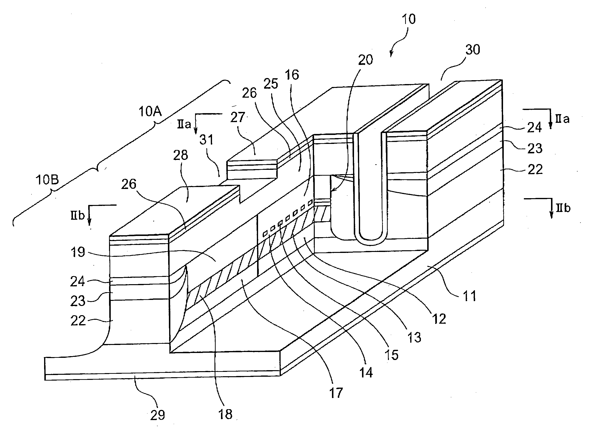
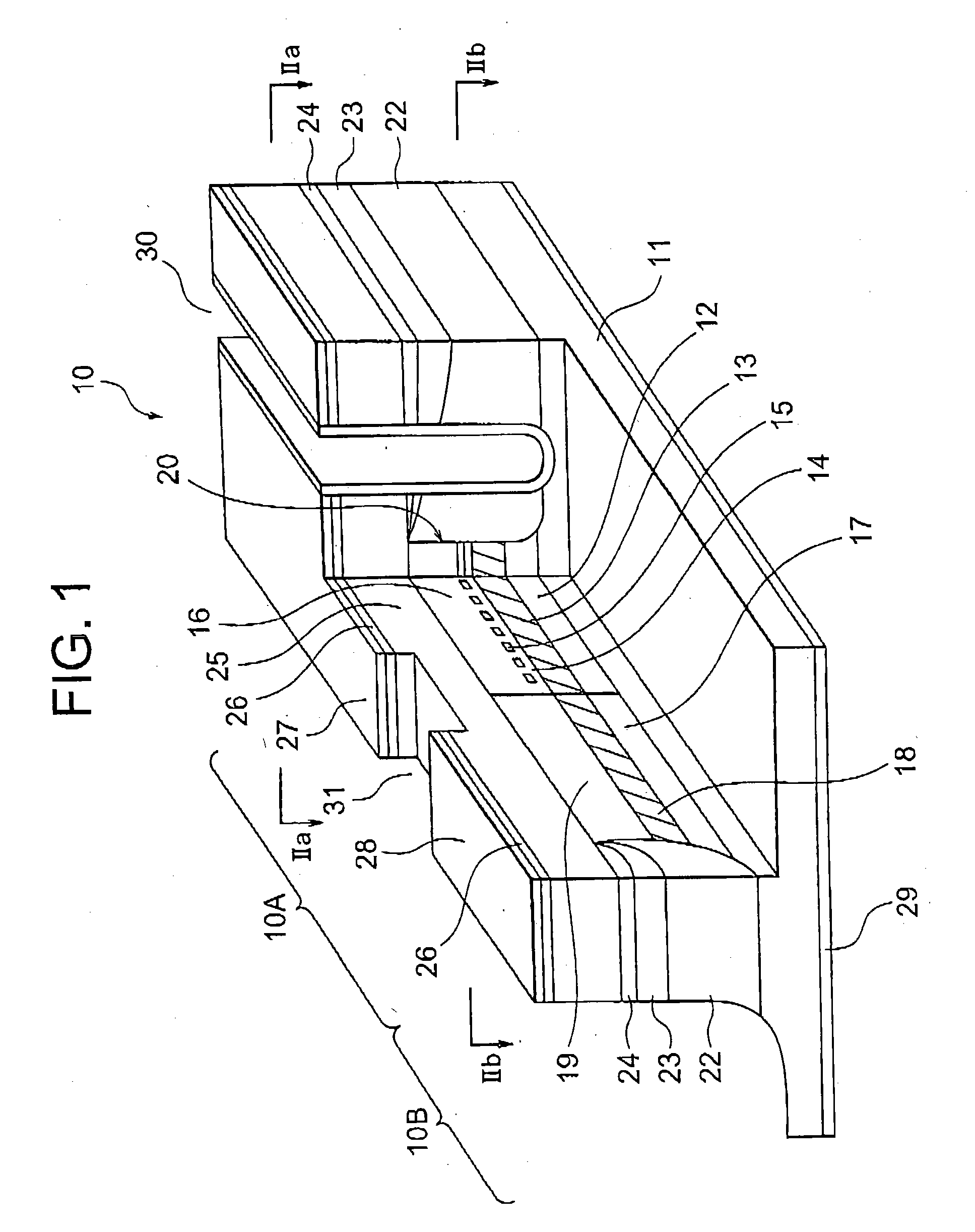
[0037] Referring to FIG. 1, an EA-DFB module generally designated by numeral 10 is of a SI-PBH type and includes a Fe--InP layer acting as an electron trapping layer in an EA modulator according to an embodiment of the present invention. The EA-DFB module 10 includes a DFB laser diode formed in the DFB laser area 10A and the EA modulator formed in the EA modulator area 10B, which are integrated in a monolithic structure and coaxially arranged on a common n-InP substrate 11 in the direction of axis of the optical waveguide.

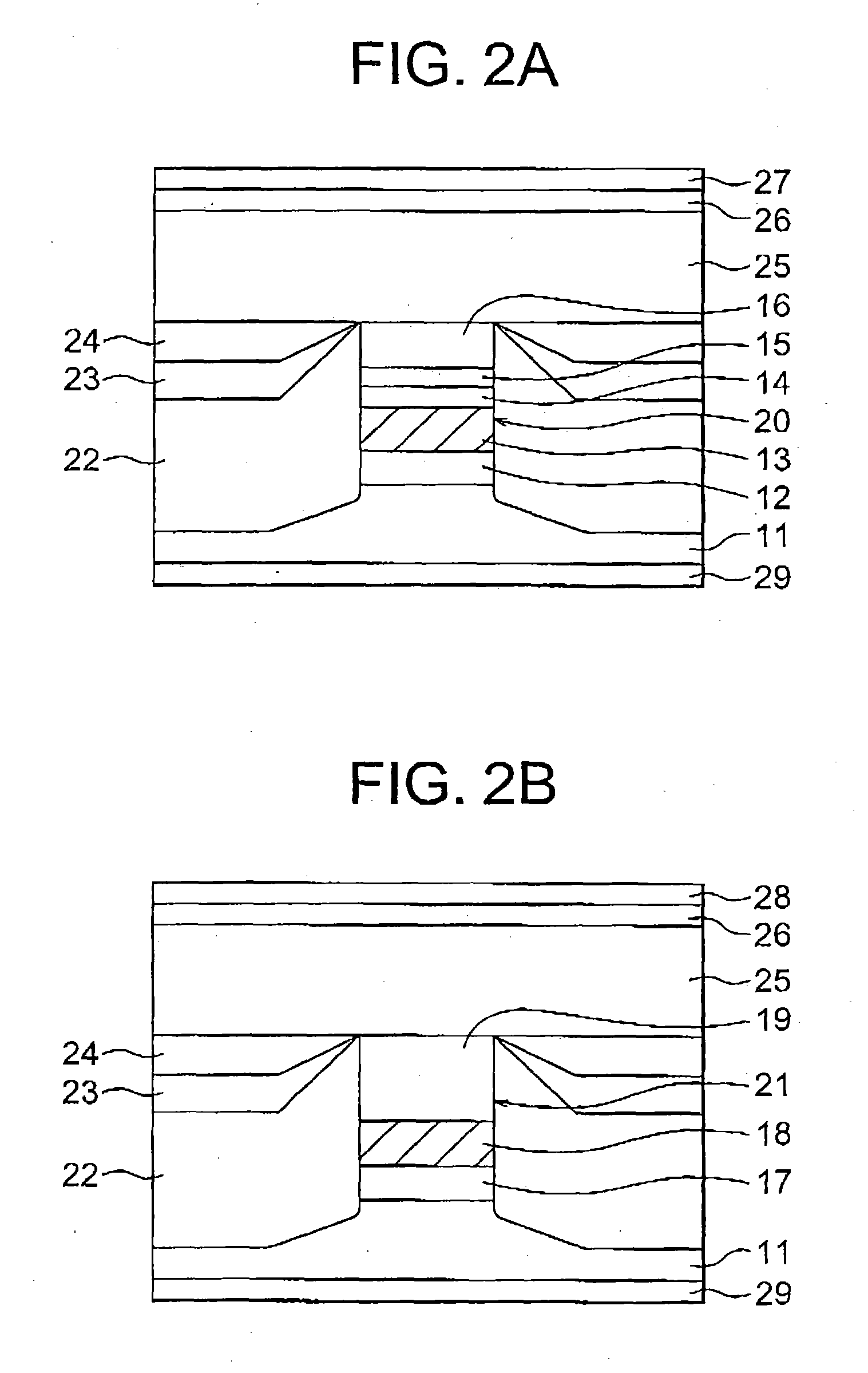
[0038] The DFB laser area 10A, as shown in FIG. 2A, has a layer structure including an n-InP lower cladding layer 12, a MQW-SCH active layer structure 13, p-InP spacer layer 14, a diffraction grating 15, and a p-InP upper cladding layer 16, which are consecutively formed on the n-InP substrate 11. Among the layers in the layer structure of the DFB laser area 10A...


PUM


Abstract

An EA-DFB module including a DFB laser diode and an EA modulator formed on an InP first-conductivity-type substrate has a mesa stripe, a current blocking structure formed on both side surfaces of the mesa strip and a second InP cladding layer formed on top of the mesa stripe and the current blocking structure. The current blocking structure includes a Fe-doped semi-insulating film, a first conductivity-type buried layer and a carrier-depleted layer. The carrier-depleted layer reduces the parasitic capacitance at the boundary between the first-conductivity-type buried layer and the second InP cladding layer.

Description

[0001] (a) Field of the Invention[0002] The present invention relates to an optical device having a carrier-depleted layer.[0003] (b) Description of the Related Art[0004] An optical integrated device including a distributed-feedback (DFB) laser diode and an electro-absorptive optical modulator (referred to as simply EA modulator hereinafter) is generally referred to as EA-DFB module or EAML (electro-absorptive-modulated laser) module. The EA-DFB modulator has advantages over the conventional optical device having an external optical modulator in that the EA-DFB module has a smaller occupied area and can be fabricated with a lower cost. Thus, the EA-DFB module attracts more attention in the field of wavelength-division-multip-lexing communication system. In particular, the EA-DFB module is noticed as a key device for implementing a light source in a metropolitan optical communication system.[0005] The EA modulator includes an absorption layer having a quantum well structure, and uses...

Claims


Application Information

Patent Timeline
IPC IPC(8): H01S5/026G02F1/017H01S5/12H01S5/22H01S5/34H01S5/343
CPCB82Y20/00H01S5/0265H01S5/12H01S5/2222H01S5/34306H01S5/2226H01S5/3072H01S5/3409H01S5/2224
Inventor IKEDA, NARIAKIYAMAGUCHI, TAKEHARUARAKAWA, SATOSHIYAMANAKA, NOBUMITSUKASUKAWA, AKIHIKONAKASAKI, RYUSUKE
Owner FURUKAWA ELECTRIC CO LTD
Why Eureka
Try Eureka