Clamp circuit

a technology of clamping circuit and clamping plate, which is applied in the direction of pulse manipulation, pulse technique, instruments, etc., can solve the problems of lowering the response speed, raising the production cost of the clamping circuit, and the inability to employ the low withstand voltage device process,

Inactive Publication Date: 2004-04-29
DENSO CORP
View PDF7 Cites 49 Cited by
  • Summary
  • Abstract
  • Description
  • Claims
  • Application Information

AI Technical Summary

Problems solved by technology

However, if the control IC 3 receives a larger number of input signals, the required number of the Zener diodes become larger, thereby increasing an area of the control substrate 1 and raising a production cost of the clamp circuit.
Accordingly, the low withstand voltage device process can not employed, but a high withstand vol

Method used


Image

  • Clamp circuit
  • Clamp circuit
  • Clamp circuit

Examples


Embodiment Construction

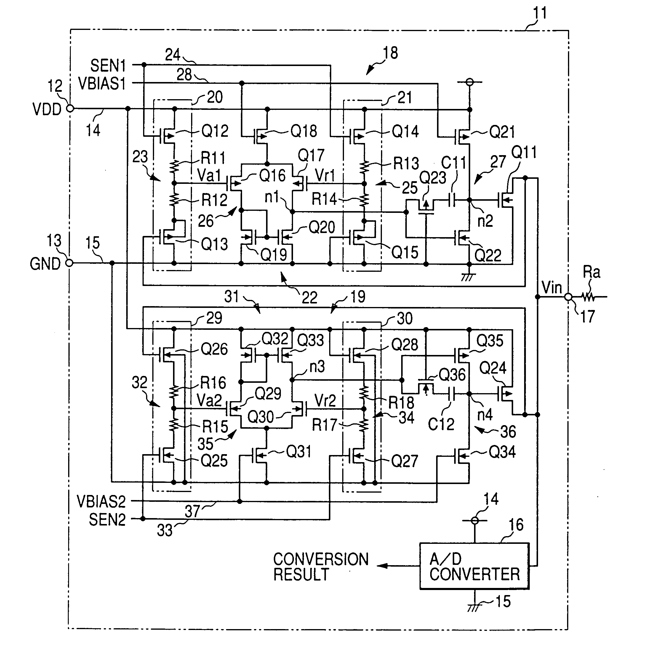
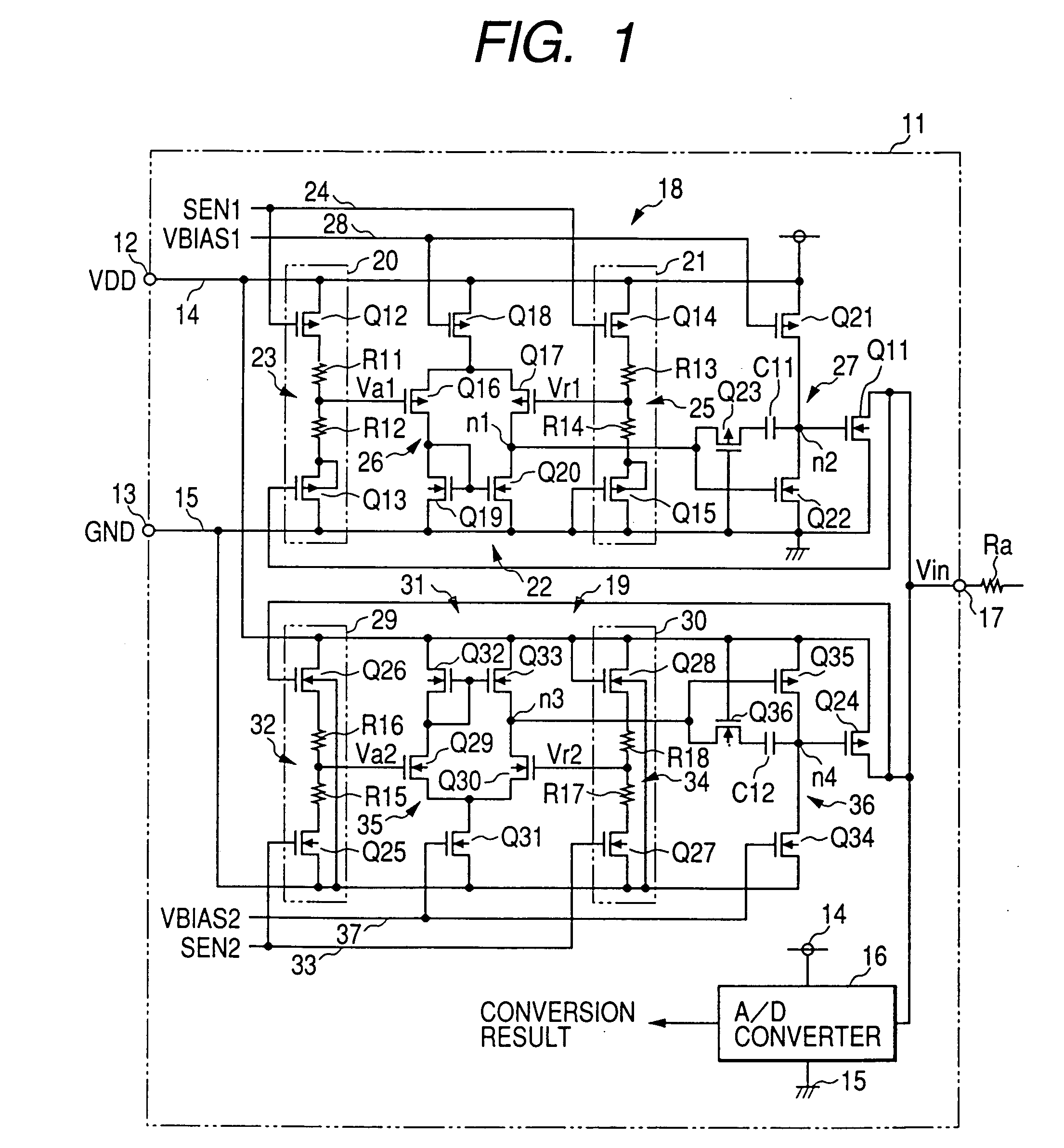
[0024] A preferred embodiment in accordance with the present invention are disclosed in detail, referring to FIG. 1 which shows a semiconductor IC for preventing a positive and negative overvoltage which might be caused by the voltages inputted into a semiconductor IC 11 mounted on a not-shown control substrate in an electronic control unit (ECU).

[0025] There is also mounted on the not-shown control substrate a not-shown power supply IC which allows the IC 11 to operate under V.sub.DD supplied through supply terminals 12 and 13 from the not-shown supply IC. Here, An accuracy of V.sub.DD is, e.g., 5 V.+-.5%. The supply terminals 12 and 13 are connected inside the IC 11 with a higher voltage supply line 14 and lower voltage supply line 15, repectively.

[0026] Althroug the IC 11 manufactured by the CMOS process includes not-shown various analog and digital circuits, only an A / D converter 16 is shown in FIG. 1. The higher voltage is e.g., 5.5 V and the lower voltage is e.g., minus 0.5 V,...


PUM


Abstract

The clamp circuit clamps an input voltage at prescribed higher and lower clamp voltages which are stabilized under a temperature fluctuation. Transistors Q12 and Q14 are switched on in their linear region. In a lower voltage clamp circuit 18, an Vin detecting circuit 20 outputs Va1 by level-shifting Vin by Q13 and voltage-divides by series resistance circuit 23 the level-shifted Vin, while a reference voltage generating circuit 21 outputs Vr1 by level-shifting 0 V by Q15 and voltage-divides by series resistance circuit 25 the level-shifted voltage. Q11 is switched on, when a comparator 22 determines that Va1 descends and goes across Vr1. Here, Q12 is of the same characteristics as Q14, while Q13 is of the same characteristics as Q15. Further, the resistance of the circuits 23 is the same as that of the circuit 25. The higher voltage clamp circuit 19 is similar to the circuit 18.

Description

[0001] 1. Field of the Invention[0002] The present invention relates to a clamp circuit for clamping a voltage inputted into a signal input terminal in a semiconductor integrated circuit (IC).[0003] 2. Description of the Related Art[0004] Recently, a large scale semiconductor IC (LSI) is manufactured in a smaller scale rule, in order to raise a response speed of the device and to reduce its chip area. Accordingly, for example, a thickness of a gate oxide film is made thinner, thereby causing such a necessity that a gate voltage be lower in order to ensure a sufficient device life and therefore, any overvoltage not be applied to the device in order to prevent a device destruction.[0005] In order to lower the gate voltage, it is effective to employ a step-down circuit mainly used in an internal logic circuit in LSI for lowering a supply voltage. Further, in order to avoid an application of the overvoltage, it is effective to add a clamp circuit to a buffer circuit or interface circuit...

Claims


Application Information

Patent Timeline
IPC IPC(8): G05F3/24H01L21/822H01L27/04H03G11/00
CPCG05F3/242H03K5/08
Inventor NODA, SHINICHIISHIHARA, HIDEAKISUZUKI, AKIRA
Owner DENSO CORP
Why Eureka
Try Eureka