Method of fabricating heterojunction photodiodes integrated with cmos

a photodiode and heterojunction technology, applied in the field of fabricating heterojunction photodiodes integrated with cmos, can solve the problems of inability to detect "solar blind" ultra-violet detection, low efficiency of both devices in near infra-red detection, and low efficiency of both devices, so as to reduce the lateral dimension and reduce the mass

Inactive Publication Date: 2004-05-20
QUANTUM SEMICON
View PDF6 Cites 79 Cited by
  • Summary
  • Abstract
  • Description
  • Claims
  • Application Information

AI Technical Summary

Benefits of technology

[0025] Yet another object of the invention is to provide a method of fabricating light sensing devices integrated with CMOS circuitry, that are ideally suited for operation in avalanche mode, with many advantages and none of the drawbacks of the conventional APDs.
[0058] Briefly, there are many advantages to the fabrication of very large two-dimensional arrays of light sensors according to the present invention.

Problems solved by technology

Also for that reason both devices have very low efficiency of near Infra-Red (IR) detection, and are incapable of detection of the 1.3 .mu.m and 1.55 .mu.m wavelengths, which are used for fiber optics communications.
Yet again for that same reason both devices cannot provide "solar blind" Ultra-Violet (UV) detection.
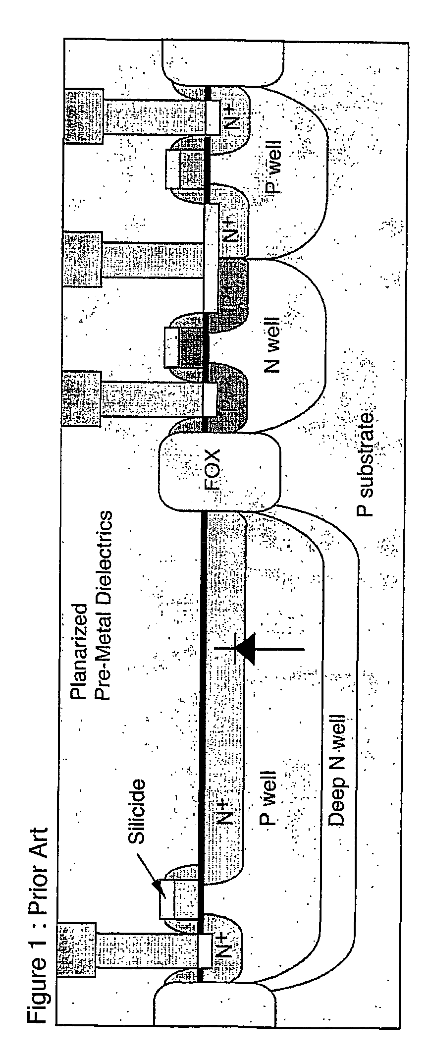
However, it is becoming evident that for advanced CMOS technologies (e.g. below 0.25 .mu.m) there are fundamental issues that prevent a modular straightforward integration of image sensors with standard CMOS logic.
At the present time, all evidence leads to the conclusion that the problems of integrating light sensors with standard CMOS becomes worse as the critical dimensions become smaller (more advanced CMOS technology).
The scaling of CMOS imagers faces two types of issues: semiconductor physics and technological problems.
The semiconductor physics problem is related to the thickness (depth) of silicon necessary to absorb enough light in order to produce a useful electrical signal.
On the other hand, it is also a technological issue because the depth of trench isolation between CMOS devices, and the source / drain junctions become shallower with each new, more advanced, CMOS generation.
When the depth of the isolation trenches becomes less than the distance required to absorb photons of a particular wavelength, then it is no longer possible to separate the charge carriers generated by light penetrating silicon at adjacent pixels.
Consequently, there is a loss of resolution for the detection of that color.
However, these extra process steps do not address the photodiode device architecture and / or materials, which remains unchanged.
With these modifications the fabrication of image sensors is no longer modular and requires extended adjustments for every new CMOS generation.
At the moment, optoelectronic transceivers for fiber optics communications, consisting of a light sensing device (photodiode) and trans-impedance amplifiers, are made with different III / V compound materials, and are not made monolithically integrated.
Alternative device architectures for light sensing do exist, but fail to fulfill all the necessary requirements for manufacturable high quality photo-detection in the visible or invisible range, or have not been able to compete with standard straightforward CCDs and CMOS imagers.
However, for reasons related to the quality of the active-layer material (ion-implanted bulk silicon), and for other reasons related to the device architecture (bulk lateral pn-photodiode) this kind of APD has not, and is not likely, to succeed in competing against CCDs and CMOS imagers.
Avalanche mode is not a viable option with conventional CMOS light sensors because the avalanche mode requires the depletion region of the pn-junction to be under an electric field near the breakdown field of the junction, which for silicon is close to 500 kV / cm.

Method used


Image

  • Method of fabricating heterojunction photodiodes integrated with cmos
  • Method of fabricating heterojunction photodiodes integrated with cmos
  • Method of fabricating heterojunction photodiodes integrated with cmos

Examples


Embodiment Construction

[0071] The present invention is based on the following knowledge. For active media made of bulk semiconductor materials, that is, without quantum confinement in any of the three spatial directions, the absorption depth for a given photon energy or wavelength (color) is determined by the band-structure of the bulk material.

[0072] The absorption efficiency of a semiconductor material for photons varies as a function of wavelength. For wavelengths around 650 nm, the coefficient of absorption of germanium is about 50 times larger than that of silicon, or conversely, for that wavelength, the same amount of light can be absorbed in a Ge film 50 times thinner than in Si (S. M. Sze, "Physics of Semiconductor Devices", Wiley, New York 1981, p.750, FIG. 5).

[0073] It is known that the absorption properties of a given semiconductor material can be changed by alloying with other materials and / or by "quantization effects" resulting from "reduced dimensionality" in at least one spatial direction. ...


PUM


Abstract

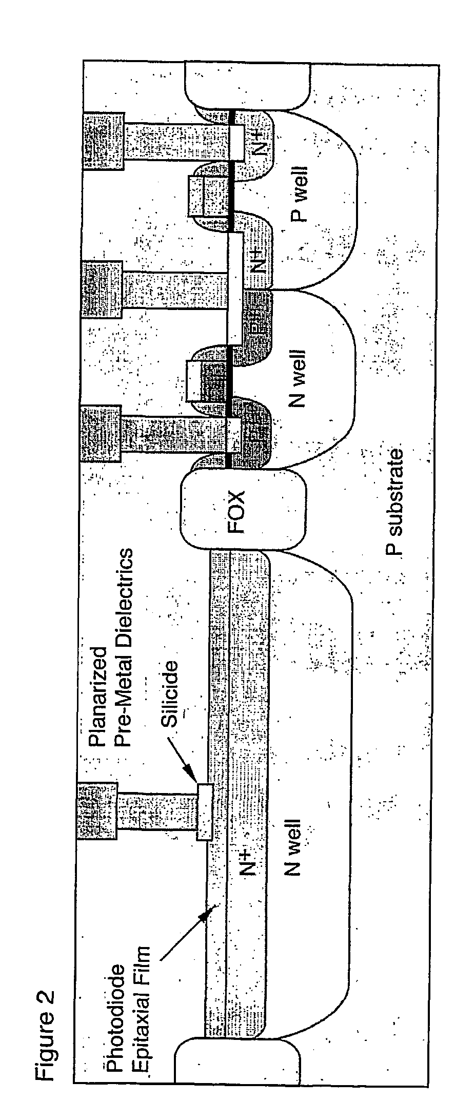
A method in which thin-film p-i-n heterojunction photodiodes are formed by selective epitaxial growth / deposition on pre-designated active-area regions of standard CMOS devices. The thin-film p-i-n photodiodes are formed on active areas (for example n<+>-doped), and these are contacted at the bottom (substrate) side by the "well contact" corresponding to that particular active area. There is no actual potential well since that particular active area has only one type of doping. The top of each photodiode has a separate contact formed thereon. The selective epitaxial growth of the p-i-n photodiodes is modular, in the sense that there is no need to change any of the steps developed for the "pure" CMOS process flow. Since the active region is epitaxially deposited, there is the possibility of forming sharp doping profiles and band-gap engineering during the epitaxial process, thereby optimizing several device parameters for higher performance. This new type of light sensor architecture, monolithically integrated with CMOS, decouples the photo-absorption active region from the MOSFETs, hence the bias applied to the photodiode can be independent from the bias between the source, drain, gate and substrate (well) of the MOSFETs.

Description

[0001] The present invention relates to the fabrication of light-sensing devices based on, and integrated with, silicon Complementary Metal Oxide Semiconductor (CMOS) circuits.[0002] There are two main light-sensor architectures in silicon technology: Charge Coupled Devices (CCDs), whose operation is based on MOS diodes, and CMOS image sensors whose operation is based on pn-junctions. The principles of operation of these devices can be found in "Physics of Semiconductor Devices" by S. M. Sze, Wiley, New York, 1981, Chapters 7 and 13.[0003] For both device types the absorption efficiency as a function of wavelength is entirely dependent on the optoelectronic properties of bulk silicon. For that reason, both device types have significantly different responses for wavelengths at the extremes of the visible spectrum (violet / blue versus red). Also for that reason both devices have very low efficiency of near Infra-Red (IR) detection, and are incapable of detection of the 1.3 .mu.m and 1....

Claims


Application Information

Patent Timeline
Patent Type & Authority Applications(United States)
IPC IPC(8): H01L21/00H01L21/8249H01L27/146H01L31/10H04N5/335
CPCB82Y20/00H01L27/14609H01L27/14621H01L27/14632H01L27/14692H01L27/14643H01L27/14687H01L27/14689H01L27/14636
Inventor AUGUSTO, CARLOS J.R.P.FORESTER, LYNN
Owner QUANTUM SEMICON
Why Eureka
Try Eureka