Semiconductor package substrate having bonding pads with plated layer thereon and process of manufacturing the same

a technology of semiconductor package substrate and bonding pad, which is applied in the manufacture of printed circuits, conductive pattern reinforcements, basic electric elements, etc., can solve the problems of poor soldering strength, insufficient soldering strength, and large challenges faced by semiconductor package manufacturers, and achieve the effect of increasing the reliability of the semiconductor packag

Inactive Publication Date: 2004-05-27
PHOENIX PRECISION TECH CORP
View PDF1 Cites 56 Cited by
  • Summary
  • Abstract
  • Description
  • Claims
  • Application Information

AI Technical Summary

Benefits of technology

[0012] It is another objective of the invention to provide a package substrate having a plurality of bonding pads with a plated layer thereon and a process of manufacturing the package substrate, through which problems such as non-uniform plating thickness and black pads are overcome, and the reliability of the semiconductor package is increased.
[0013] It is another objective of the invention to provide a package substrate having a plurality of bonding pads with a plated layer thereon and a process of manufacturing the package substrate in which formation of a plurality of additional plating wires on the package substrate is not required. Thereby, the available routing area is greatly increased and noise interference induced by the plating wires can be prevented.
[0014] It is another object of the invention to provide a package substrate having a plurality of bonding pads with a plated layer thereon and a process of manufacturing the package substrate in which formation of a Ni / Au layer over the whole trace layer of the substrate is not required, so that the production cost can be significantly reduced.
[0017] According to the package substrate and the manufacturing process of the invention, the plated layer (such as a Ni / Au layer) covering the exposed surface of the bonding pads of the package substrate improves the electrical connection to other devices, and protects the bonding pads from oxidizing in the ambient environment. Problems such as non-uniform plating thickness and black pads thereby are overcome, and the reliability of the semiconductor package is improved. During plating a Ni / Au layer on the bonding pads, the conductive film serves as a path for electrical current to electrically connect the bonding pads on the package substrate, without the need of plating wires on the package substrate. Thereby, the available routing area is greatly increased and noise interference induced by the plating wires is avoided. Furthermore, formation of a Ni / Au layer over the whole trace layer of the substrate, which is necessary in the prior art, is not required in the invention. Thus the production cost thereby is significantly reduced.

Problems solved by technology

Semiconductor package manufacturers have confronted great challenges to satisfy the requirements of product size reduction.
This process usually has disadvantages such as poor solderability and insufficient soldering strength, and further may form black pads and soldering with non-uniform-thickness.
Soldering with non-uniform-thickness occurs when the nickel bath varies between temperature cycles.
Even if the optimal operating conditions have been satisfied, the Gold layer often does not fully cover the nickel layer and thus the underlying copper layer may be externally exposed.
Black pads are typically formed when the substrate is dipped in a gold bath while excessive oxidation is occurring.
Problems such as non-uniform thickness and black pads deteriorate the connection and bonding of gold wires, solder bumps, presolder or solder balls to the bonding pads.
Therefore, the reliability of the semiconductor package is reduced.
However, the plating wires 11 undesirably occupy a portion of the routing area of the substrate 1, and further may generate noise due to an antenna effect when used at high frequency.
Since the material cost of the Ni / Au layer is expensive, material wastage of the Ni / Au layer increase the total production cost.
Also, the solder mask subsequently formed to cover the substrate is not very compatible with the Ni / Au layer, which further reduces the reliability.

Method used


Image

  • Semiconductor package substrate having bonding pads with plated layer thereon and process of manufacturing the same
  • Semiconductor package substrate having bonding pads with plated layer thereon and process of manufacturing the same
  • Semiconductor package substrate having bonding pads with plated layer thereon and process of manufacturing the same

Examples


first embodiment

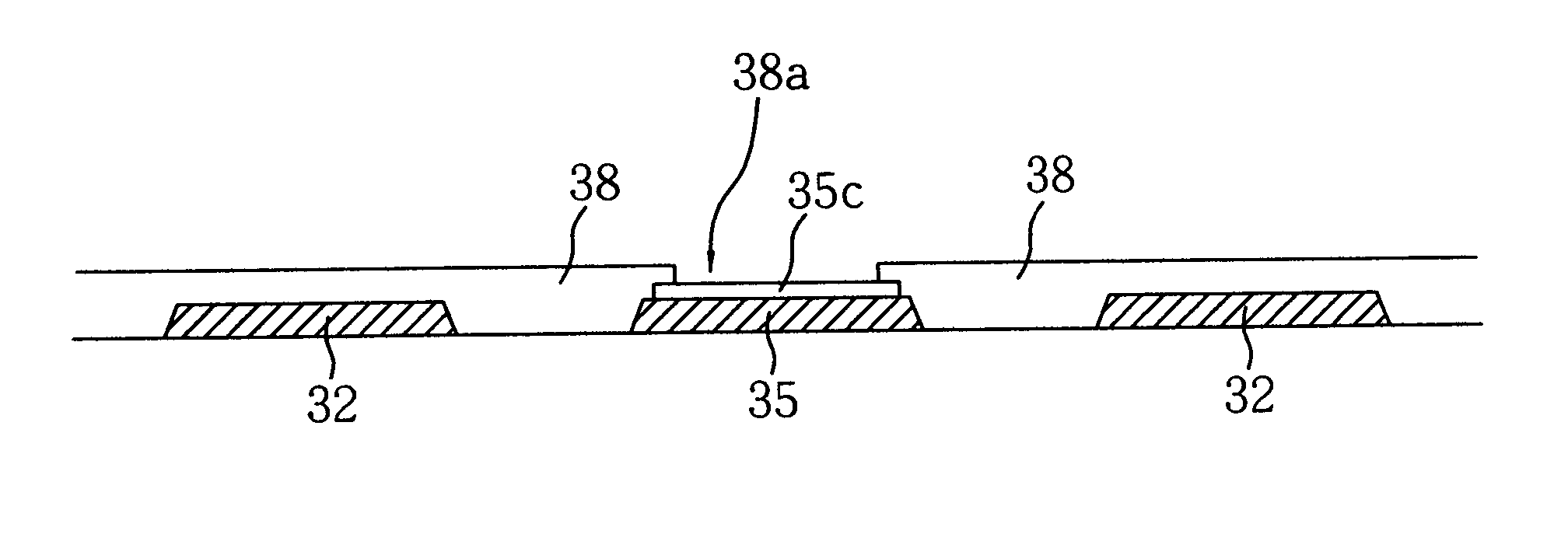
[0033] FIG. 4A to FIG. 4H are cross-sectional views of a bonding pad electrically connecting to a semiconductor package substrate according to the invention.

[0034] Referring to FIG. 4A, a semiconductor package substrate 3 is provided. The substrate 3 can be, for example, the flip-chip package substrate as shown in FIG. 3, or a wire-bonding package substrate. The substrate 3 has been previously subjected to a front-end process. For example, a plurality of plated through holes or blind vias have been formed through the substrate 3. The trace layers 32 have been formed on the substrate 3. The trace layers 32 further may include a plurality of bonding pads 35. The process of forming the above parts is well known in the art, and its description is omitted herein.

[0035] Referring to FIG. 4B, a conductive film 36 is formed over the substrate 3. The conductive film 36 serves as electric current paths for electroplating the metal layer 35c. The conductive film 36 is made of a metal selected ...

second embodiment

[0040] FIG. 5A to FIG. 5I are cross-sectional views of a bonding pad formed on a semiconductor package substrate according to the invention.

[0041] Referring to FIG. 5A, a package substrate 3 is provided. The substrate 3, as describe above, can be a flip-chip package substrate 3 or a wire-bonding package substrate. The substrate 3 has been subjected to a front-end process. For example, a plurality of through holes or blind holes (not shown) are formed through the substrate 3, and at least one trace layer 32 is formed on / inside the substrate 3.

[0042] Referring to FIG. 5B, a conductive film 36 as illustrated in the first embodiment of the invention is formed over the substrate 3. The conductive film 36 serves as electric current paths for the electroplating metal layer 35c.

[0043] Referring to FIG. 5C, a photoresist layer 37 is formed by printing or coating over the substrate 3 on top of the conductive film 36 thereon. The photoresist layer 37 can be, for example a dry film or a liquid ...


PUM


Abstract

A semiconductor package substrate is provided having a plurality of bonding pads on at least one surface thereof and covered by a conductive film. A photoresist layer formed over the conductive film has a plurality of first openings for exposing portions of the conductive film corresponding to the bonding pads. The exposed portions of the conductive film is removed to expose the bonding pads respectively via the first openings. The exposed bonding pads are plated with a metal layer respectively. Then, the photoresist layer and the remainder of the conductive film covered by the photoresist layer are removed. A solder mask having a plurality of second openings may be formed on the surface of the substrate, and allows the plated metal layer on the bonding pads respectively to be exposed via the second openings.

Description

[0001] 1. Field of the Invention[0002] The invention relates to a semiconductor package substrate having a plurality of bonding pads with a plated layer thereon, and a process of manufacturing the substrate. More particularly, the invention relates to a semiconductor package substrate in which a Ni / Au plated layer is formed on an exposed surface of a bonding pad, and a process of forming the Ni / Au plated layer on the exposed surface of the bonding pad of the semiconductor package substrate.[0003] 2. Description of the Related Art[0004] Semiconductor package manufacturers have confronted great challenges to satisfy the requirements of product size reduction. A plurality of conductive traces, made of copper, for example, are formed on a substrate of a semiconductor package, and respectively extend to a plurality of bonding pads for signal and electrical current transmission. A Ni / Au layer is usually formed over the exposed surface of each bonding pad to improve electrical connection b...

Claims


Application Information

Patent Timeline
Patent Type & Authority Applications(United States)
IPC IPC(8): H01L21/48H01L21/60H01L23/498H01L23/50H05K3/24
CPCH01L21/4846H01L2924/014H01L23/50H01L24/11H01L24/16H01L2224/13099H01L2224/16H01L2924/01022H01L2924/01029H01L2924/01046H01L2924/01047H01L2924/01078H01L2924/01079H01L2924/01082H01L2924/15311H05K3/243H05K2203/0361H05K2203/0542H01L2924/01024H01L23/49822H01L2924/12042H01L2224/45144H01L2924/00014H01L2924/00H01L2224/0401
Inventor CHU, CHIH-LIANGCHOU, E-TUNGWONG, LIN-YIN
Owner PHOENIX PRECISION TECH CORP
Why Eureka
Try Eureka