Cold cathode type flat panel display
a flat panel display and cold cathode technology, applied in the direction of instruments, discharge tubes, tubes with screens, etc., can solve the problems of a drop in yield or an increase in production costs, and achieve the effect of inexpensive production
- Summary
- Abstract
- Description
- Claims
- Application Information
AI Technical Summary
Benefits of technology
Problems solved by technology
Method used
Image

Examples
example 1
[0091] An example according to the first aspect of the present invention will be described with reference to FIGS. 3 to 33.
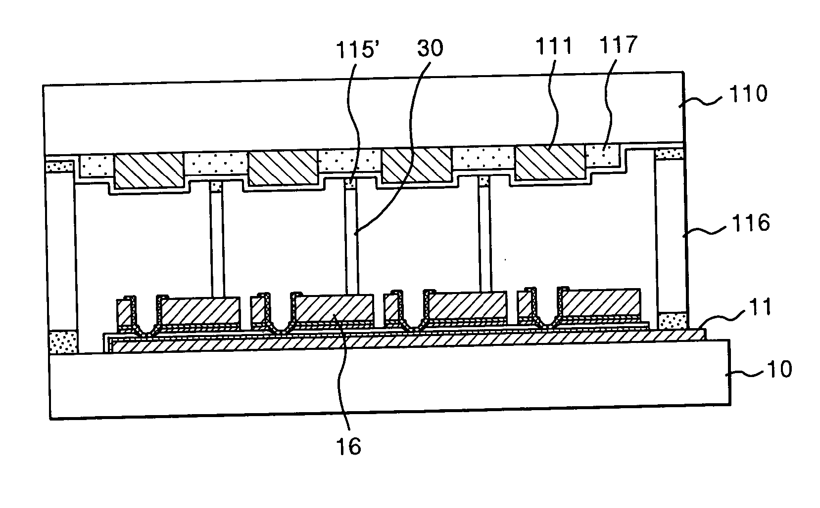
[0092] (1) Formation of a cathode substrate 10:
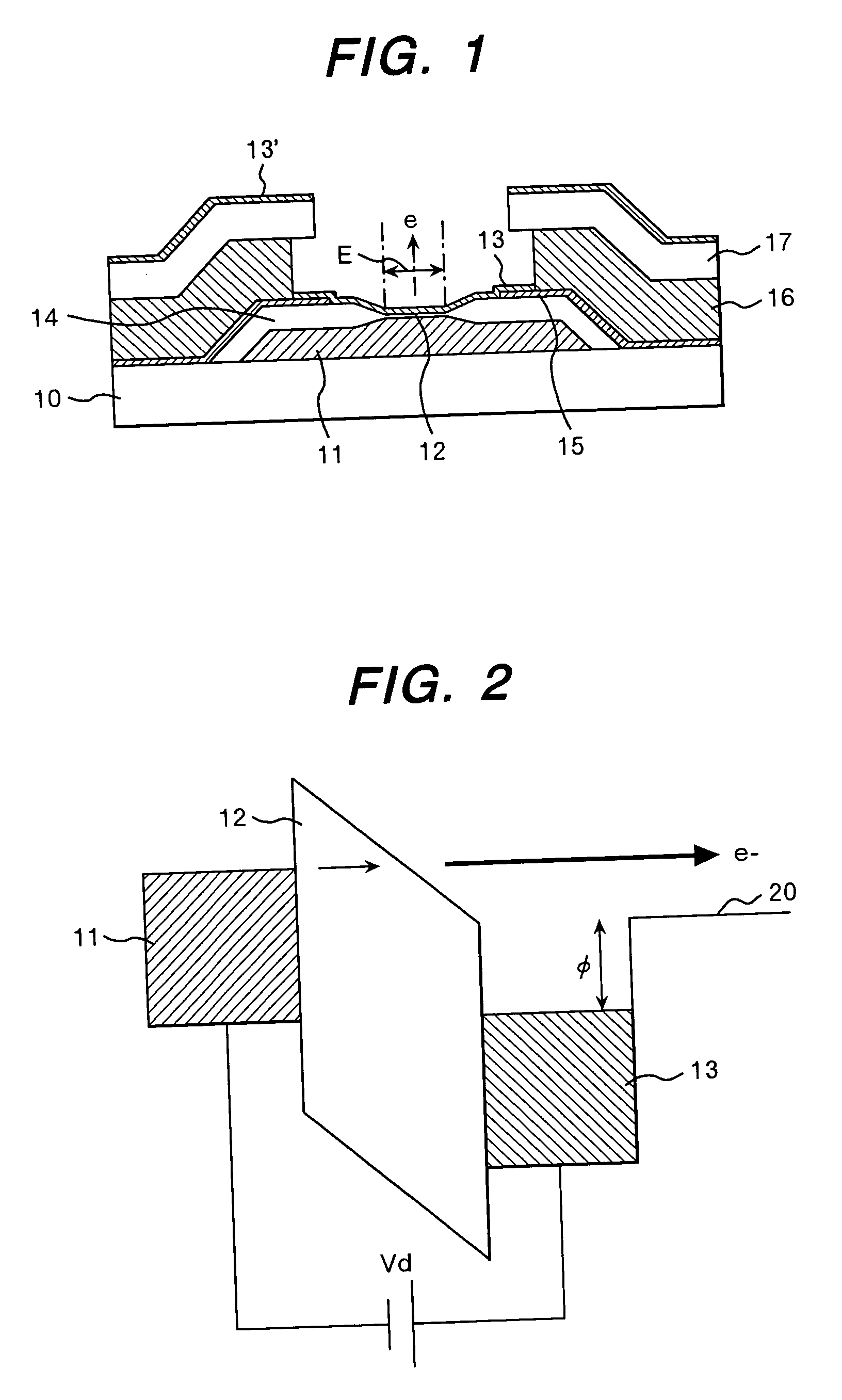
[0093] This item describes a production process in a case in which top electrodes 13 are connected electrically to contact electrodes 15 and further top electrode bus lines 16 are backed with aluminum, aluminum alloy, or a metal having a lower resistivity than aluminum.
[0094] It is beforehand stated that the MIM electron source producing process which can be used in the present invention is not limited to the present example. The present invention can easily be applied to MIM electron sources disclosed in Patent Documents 1 and 2 (Japanese Patent Application Laid-Open Nos. 2001-101965 and 2000-208076), which comprise top electrode bus lines having a tapered structure, and other MIM electron sources.
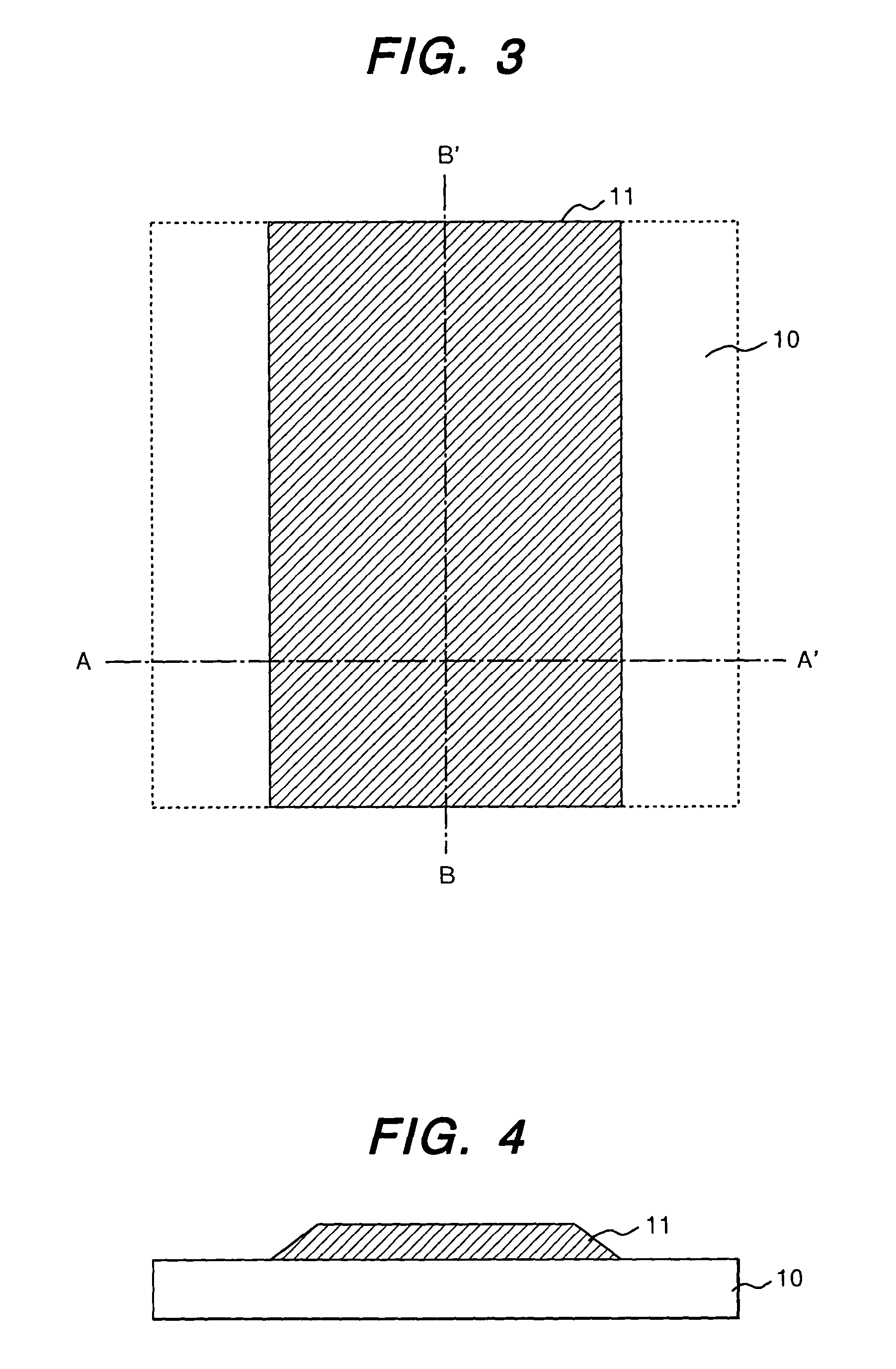
[0095] First, a metal film for bottom electrodes 11 is deposited on an insulating cathode substrate 10 made of glass or...
example 2
[0138] This example discloses a manner that ground voltage is applied to the spacer lines 16' without being passed through the scan line driver circuit 50. First, according to Example 1, the cathode substrate 10 comprising MIM electron sources, the anode substrate 110 and the panel 120 are formed.
[0139] FIG. 34 is a connection diagram illustrating the display device panel 120, which is formed as described above, connected to driver circuits. The bottom electrodes 11 are connected to the data line driver circuit 40 through the FPC 70, and the top electrode bus lines 16 are connected to the scan line driver circuit 50 through the FPC 70.
[0140] In the same way, the spacer lines 16' are connected to the scan line driver circuit 50 through the FPC 70. The FPC 70 used herein is made up to a circuit having internal lines for short-circuiting all of the spacer lines 16' in advance. In a terminal portion of the FPC 70, the unified spacer lines are connected to a ground line independently of ...
example 3
[0142] This example discloses another manner that ground voltage is applied to the spacer lines 16' without being passed through the scan line driver circuit 50. First, according to Example 1, the cathode substrate 10 comprising MIM electron sources, the anode substrate 110 and the panel 120 are formed.
[0143] In this case, attention should be paid to the matter that in the cathode substrate 10 terminals of the spacer lines 16' are extended to the outside of the top electrode bus lines 16 so as to be mutually short-circuited, which is different from Example 2.
[0144] FIG. 35 is a connection diagram illustrating the display device panel, which is formed as described above, connected to driver circuits. The bottom electrodes 11 are connected to the data line driver circuit 40 through the FPC 70, and the top electrode bus lines 16 are connected to the scan line driver circuit 50 through the FPC 70. The spacer lines 16' are unified at one end of the cathode substrate and on the cathode su...
PUM
 Abstract
Description
Claims
Application Information
 - R&D
- Intellectual Property
- Life Sciences
- Materials
- Tech Scout
- Unparalleled Data Quality
- Higher Quality Content
- 60% Fewer Hallucinations
Browse by: Latest US Patents, China's latest patents, Technical Efficacy Thesaurus, Application Domain, Technology Topic, Popular Technical Reports.
© 2025 PatSnap. All rights reserved.Legal|Privacy policy|Modern Slavery Act Transparency Statement|Sitemap|About US| Contact US: help@patsnap.com