Method of forming cavity between multilayered wirings

a multi-layered wiring and cavity technology, applied in the direction of semiconductor/solid-state device details, coatings, solid-state devices, etc., can solve the problems of difficult to obtain low-dielectric constant films, and difficulty in obtaining the film strength necessary for semiconductor device formation processing

Inactive Publication Date: 2004-07-08
JSR CORPORATIOON
View PDF2 Cites 26 Cited by
  • Summary
  • Abstract
  • Description
  • Claims
  • Application Information

AI Technical Summary

Problems solved by technology

However, since relatively minute films are obtained by the CVD process, it is difficult to obtain a low dielectric constant of 2.5 or less.
According to realization of a high porosity of SOG, since the dielectric constant increases with an increase in hygroscopicity following the realization of a high porosity, the effect of realizing a low dielectric constant by a reduction of film density is cancelled so that it is difficult to obtain low-dielectric constant films.
While dielectric films with a low dielectric constant containing a polyorganosiloxane as the major component and called organic SOG are developed, in the case where it is intended to obtain a low dielectric constant of 2.3 or less, there is a problem such that a film strength necessary for formation processing of semiconductor devices is not obtained.
However, according to those conventional methods, after preparing a structure in which a space between metallic wirings is filled with an organic resist or a silica compound, the organic resist or the silica compound is removed by etching or icing to form a cavity between the metallic wirings, and hence, there was involved a problem such that the operation is complicated.

Method used


Image

  • Method of forming cavity between multilayered wirings
  • Method of forming cavity between multilayered wirings
  • Method of forming cavity between multilayered wirings

Examples


example 1

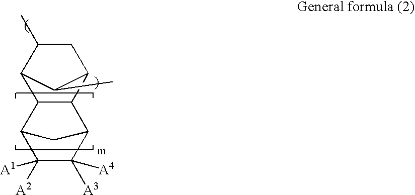
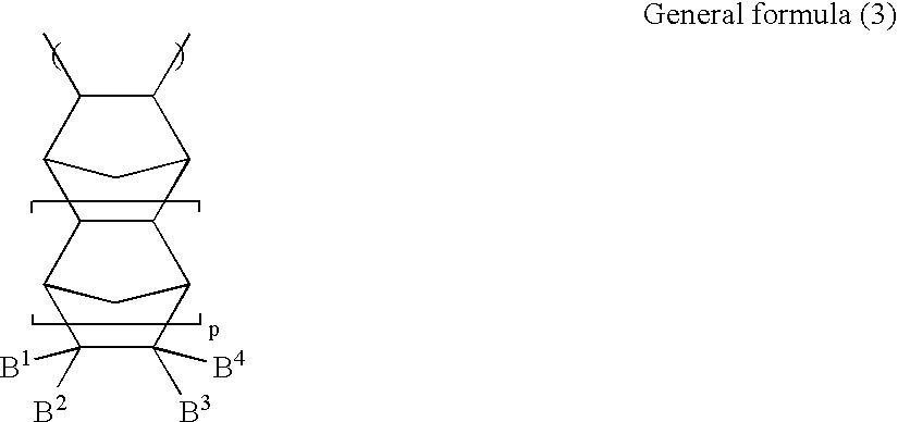
[0277] 47 g (500 mmoles) of bicyclo[2.2.1]hept-2-ene, 66 g (500 mmoles) of endo-tricyclo[5.2.1.0.sup.2,6]deca-3,8-diene, 0.42 g (5 mmoles) of 1-hexene, and 480 g of toluene and 85 g of cyclohexane as solvents were placed in a 2 liters stainless steel-made reactor under nitrogen.

[0278] A solution of nickel octanoate in hexane and hexafluoroantimonic acid were reacted in a molar ratio of 1 / 1 at -10.degree. C., a precipitate of nickel bis(hexafluoroantimonate) [Ni(SbF.sub.6).sub.2] formed as a by-product was removed by filtration, and the residue was diluted with toluene. The resulting hexafluoroantimonic acid modified material of nickel octanoate (0.40 mmoles as a nickel atom), 1.2 mmoles of boron trifluoride ethyl etherate, 8.0 mmoles of methyl alumoxane, 0.4 mmoles of 1,5-cyclooctadiene, 8.0 mmoles of methyl triethoxysilane were charged in the order of methyl triethoxysilane, 1,5-cyclooctadiene, methyl alumoxane, boron trifluoride ethyl etherate, and the hexafluoroantimonic acid mod...

example 2

[0283] Polymerization was carried out in the same manner as in Example 1, except for using 625 mmoles of bicyclo[2.2.1]hept-2-ene, 587 mmoles of endo-tricyclo[5.2.1.0.sup.2,6]deca-3,8-diene, and 37 mmoles of 5-triethoxysilylbicyclo[2.2.1]hept-2-ene, to obtain a copolymer B in a conversion of 62%. A proportion of the structural unit derived from endo-tricyclo[5.2.1.0.sup.2,6]deca-3,8-diene as determined from the .sup.1H-NMR spectrum was 37 mol %. A proportion of the structural unit derived from 5-triethoxysilylbicyclo[2.2.1]hept-2-ene was 3.0 mol %. (This value was calculated from a ratio of the CH.sub.2 absorption of the Si--O--CH.sub.2-- group at 3.7-4.1 ppm to the absorption of all of other protons.) The copolymer B had a number average molecular weight of 60,000 and a weight average molecular weight of 121,000 as reduced into polystyrene, with an Mw / Mn ratio being 2.0.

[0284] Hydrogenation was carried out in the same manner as in Example 1 at 120.degree. C. for 4 hours under a hyd...

example 3

[0287] Polymerization was carried out in the same manner as in Example 1, except for using 625 mmoles of bicyclo[2.2.1]hept-2-ene, 587 mmoles of endo-tricyclo[5.2.1.0.sup.2,6]deca-3,8-diene, and 37 mmoles of 5-[1',4',4'-trimethyl-2',6'-dioxa-1'-silacyclohexyl]bicyclo[2.2.1 ]hept-2-ene, to obtain a copolymer C. A conversion into the copolymer was 60%. In the copolymer C, a proportion of the structural unit derived from endo-tricyclo[5.2.1.0.sup.2,6]deca-3,8-diene as determined from the .sup.1H-NMR spectrum was 36 mol %. A proportion of the structural unit derived from 5-[1',4',4'-trimethyl-2',6'-dioxa-1'-silacyclohexyl]bicyclo--[2.2.1]hept-2-ene was 3.0 mol %. (This value was calculated from a ratio of the CH.sub.2 absorption of the Si--O--CH.sub.2-- group at 3.4-4.0 ppm to the absorption of all of other protons.) The copolymer C had a number average molecular weight of 116,000 and a weight average molecular weight of 278,000 as reduced into polystyrene, with an Mw / Mn ratio being 2.4...


PUM

PropertyMeasurementUnit
mol %aaaaaaaaaa
glass transition temperatureaaaaaaaaaa
elastic modulusaaaaaaaaaa

Abstract

A method of forming a cavity between metallic wirings using a polymer capable of revealing a specific heat resistant temperature and a specific heat decomposition temperature by having a specific repeating unit structure and a specific molecular weight range and of readily forming a cavity structure between metallic wirings in, for example, semiconductors. The method comprises a step of coating the surface of a first dielectric film formed on a semiconductor substrate with a cyclic olefin based addition polymer, a step of patterning the cyclic olefin based addition polymer as a void-forming polymer, a step of forming a metallic wiring in the pattern formed on the void-forming polymer, a step of forming a second dielectric film on the void-forming polymer containing a metallic wiring, and a step of removing the void-forming polymer between the multilayered wirings by heating to form a cavity between the metallic wirings.

Description

[0001] The present invention relates to a method of forming a cavity between metallic wirings using a polymer capable of revealing a specific heat resistant temperature and a specific heat decomposition temperature by having a specific repeating unit structure and a specific molecular weight range and of readily forming a cavity structure between metallic wirings in, for example, semiconductors.DESCRIPTION OF THE RELATED ART[0002] Hitherto, silica (SiO.sub.2) films formed by the vacuum process such as the CVD process have widely been employed as a dielectric film in semiconductors, etc. Further, coating type dielectric films containing a tetraalkoxysilane hydrolyzate as the major component and called an SOG (Spin on Glass) film are employed mainly for the purpose of flattening. In recent years, following large scale integration of semiconductor devices and the like, a demand for low-dielectric constant dielectric films is increasing for the purpose of reducing a wiring parasitic cap...

Claims


Application Information

Patent Timeline
Patent Type & Authority Applications(United States)
IPC IPC(8): C08G61/06C08F32/00C09D165/00H01L21/312H01L21/768H01L23/522
CPCC08G61/06C09D165/00H01L21/312H01L21/7682H01L2924/0002H01L23/5222H01L2924/00H01L21/02126H01L21/02118H01L21/768
Inventor KUROSAWA, TAKAHIKOSHIRATO, KAORIMARUYAMA, YOUICHIROU
Owner JSR CORPORATIOON
Why Eureka
Try Eureka