Color electroluminescent displays

Inactive Publication Date: 2004-07-15
IFIRE IP CORP
View PDF24 Cites 95 Cited by
  • Summary
  • Abstract
  • Description
  • Claims
  • Application Information

AI Technical Summary

Benefits of technology

[0094] Other features and advantages of the present invention will become apparent from the following detailed description. It should be understood, however, that the detailed description and the specific examples while indicating embodiments of the invention are given by way of illustration only, since various changes and modifications within the spirit and scope of the invention will become apparent to those skilled in the art from the detailed description.

Problems solved by technology

The optical emission from these phosphor materials must be passed through an appropriate chromatic filter to achieve the necessary color coordinates for red, green and blue sub-pixels, resulting in a loss of luminance and energy efficiency.
In general, the luminance of the red, green and blue electroluminescent phosphors that make up the sub-pixels of the display decrease at different rates and result in a shift in the color balance of the display as it ages.
These measurements, however, add complexity and cost to the manufacture and operation of the display.
If these voltages are not matched properly, the brightness ratios between red, green and blue will be incorrect.
Such matching requires precise control over the thickness and composition of the phosphor and adjacent dielectric layers within the display to the extent that manufacturing yield may be compromised.
The patterning process requires photolithographic processes involving photoresist deposition, exposure, phosphor film etching and phosphor film lift-off processes for each sub-pixel phosphor material, which involves many successive steps and leads to relatively high manufacturing costs.
The chemicals used in such photolithographic processes have to be carefully purified and their use carefully controlled to avoid damage to the typically moisture-sensitive phosphor materials during the patterning process, which can also add to the cost of display manufacture.
OLEDs, however, cannot be used to build a passive matrix, large area display having many rows of pixels with a reasonable luminance.
This limitation may be mitigated to some extent by using active matrix addressing, but the thin film transistor (TFT) array needed for active matrix addressing is, in itself, difficult to scale up and costly for large area displays with a large number of addressable rows.
In addition, ultraviolet light tends to degrade the display.

Method used


Image

  • Color electroluminescent displays
  • Color electroluminescent displays

Examples


example 1

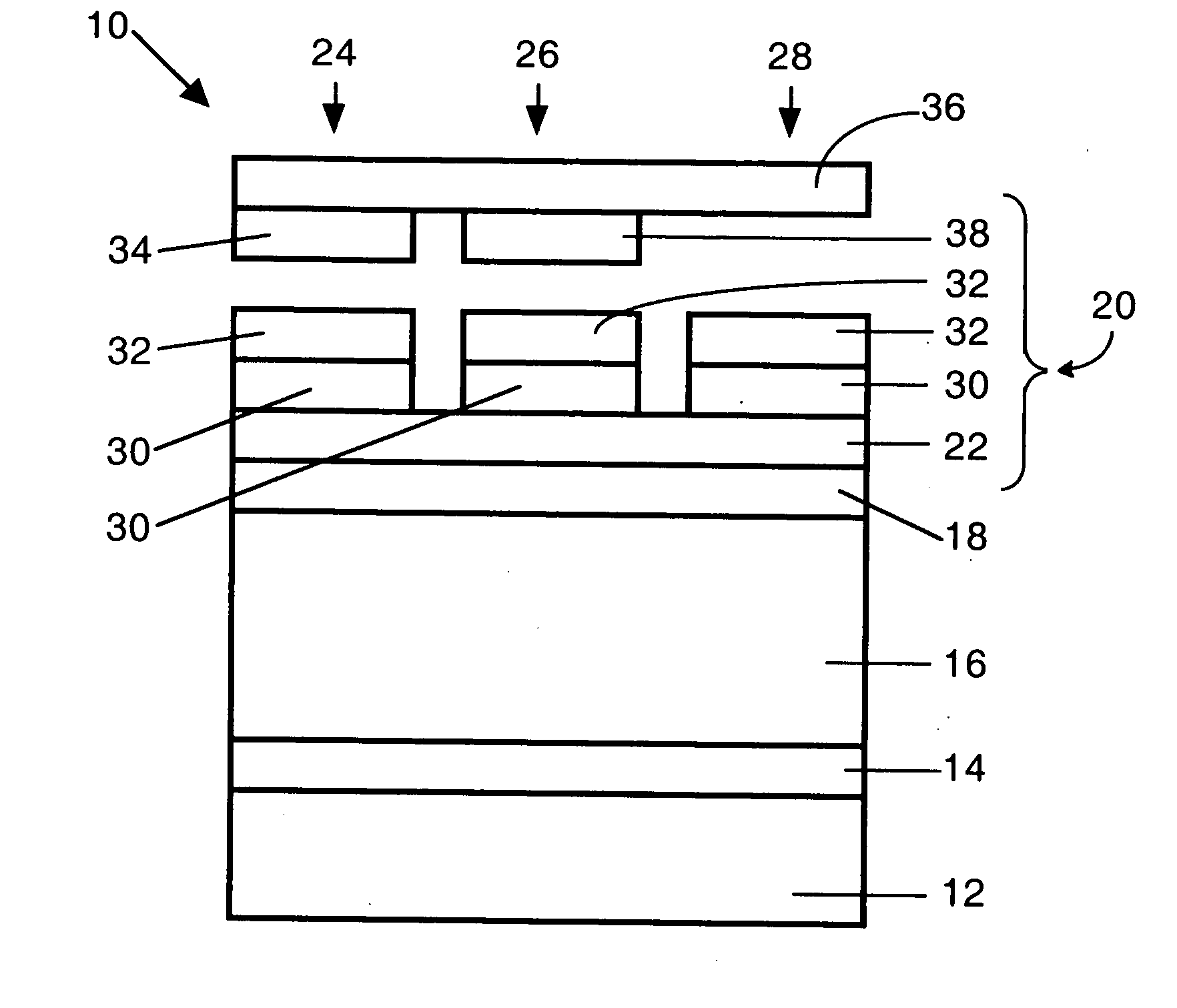
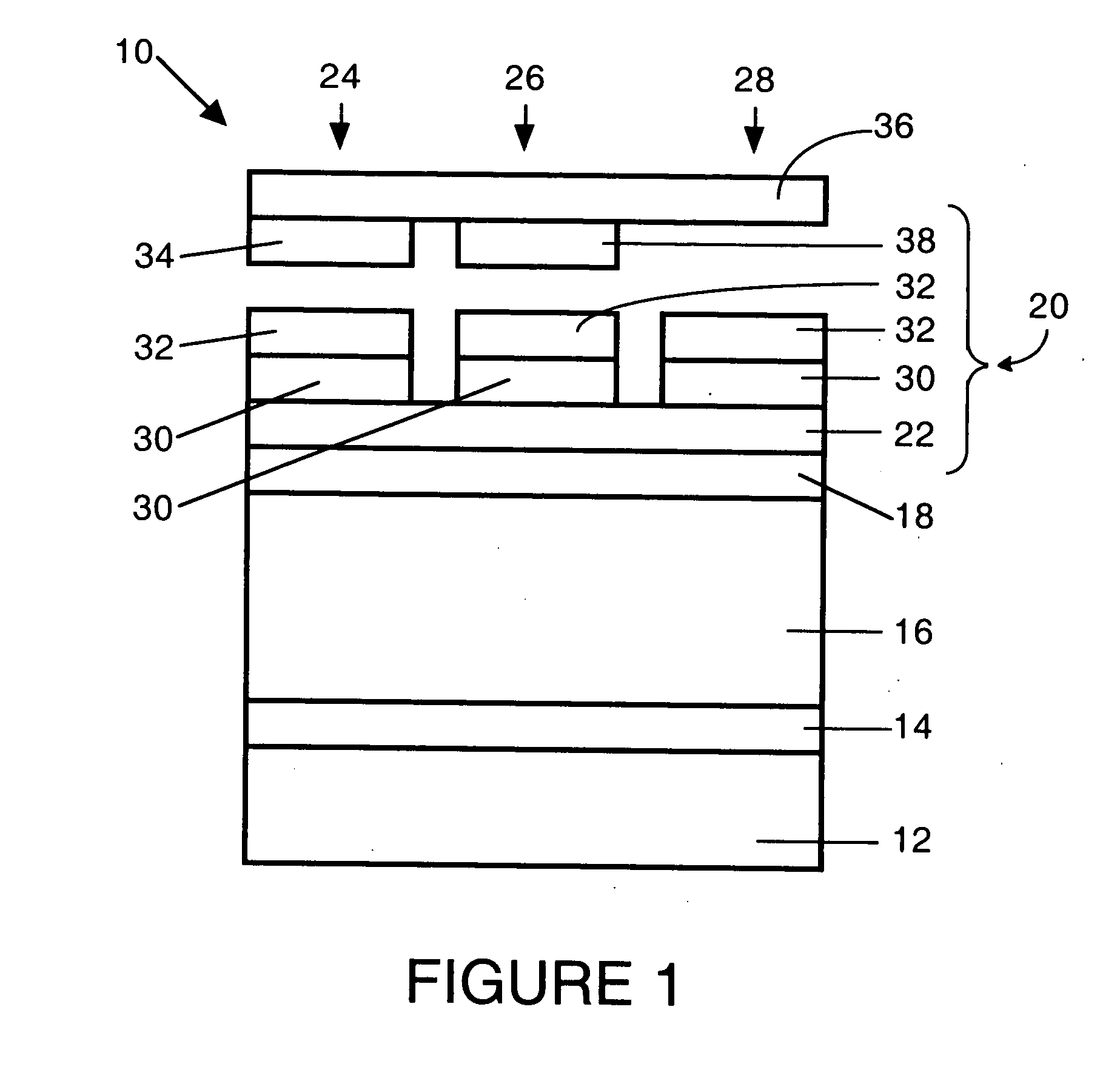
[0134] A blue-emitting electroluminescent pixel having a europium activated barium thioaluminate phosphor film was fabricated on a 5 centimeter (length).times.5 centimeter (width).times.1 millimeter (thick) alumina substrate fabricated using the methods as described in Applicant's co-pending International Patent Application PCT / CA03 / 00568 filed Apr. 17, 2003 (the disclosure of which is incorporated herein in its entirety). The pixel was operated with repetitive alternating polarity 32 microsecond wide square-wave pulses and a frequency of 120 Hz giving 240 light pulses per second. The pulse amplitude was varied. in increments of 10 volts up to 260 volts. The luminance as a function of voltage indicates a luminance at 60 volts above the threshold voltage of 100 to 150 candelas per square meter.

example 2

[0135] A solution of a green-emitting photoluminescent dye, ADS-085GE.TM. (American Dye Source Inc., Canada) was poured into a flat bottomed glass container that was placed over the pixel of Example 1. The dye solution was observed to brightly luminesce green.

example 3

[0136] A solution of a red-emitting photoluminescent dye, ADS-100RE.TM.(American Dye Source Inc., Canada) was deposited on a glass substrate and allowed to dry. It was placed with the dye layer facing the pixel of Example 1 and tested using the procedure described in Example 1. The dye was observed to brightly luminesce with a red color with no penetration of the blue exciting light through the dye.


PUM

PropertyMeasurementUnit
Thicknessaaaaaaaaaa
Sizeaaaaaaaaaa
Thicknessaaaaaaaaaa

Abstract

The present invention is directed to color electroluminescent displays comprising a novel sub-pixel structure and method for making the same. The sub-pixel structure has an electroluminescent phosphor, which emits blue light, and a photoluminescent phosphor, which emits at least one other color as a result of absorption of the blue light. The invention is also directed to novel photoluminescent phosphor materials.

Description

[0001] The present invention relates to a color electroluminescent display. More specifically, the invention relates to a color electroluminescent display wherein direct electroluminescent emission produces blue light and photoluminescent emission, initiated by absorption of the blue light, produces at least one other color.BACKGROUND TO THE INVENTION[0002] Thick film dielectric electroluminescent displays have been developed and are described, for example, in Applicant's U.S. Pat. No. 5,432,015 (the entirety of which is incorporated herein by reference). These thick film dielectric electroluminescent displays provide for superior resistance to dielectric breakdown as well as a reduced operating voltage compared to thin film electroluminescent (TFEL) displays. A thick film dielectric structure deposited on a ceramic substrate withstands higher processing temperatures and facilitates annealing of phosphor films at higher temperatures to improve their luminosity. With these advantages...

Claims


Application Information

Patent Timeline
IPC IPC(8): C09K11/06C09K11/77H01L51/50H05B33/10H05B33/14
CPCC09K11/06C09K11/7706C09K11/7707C09K11/7712Y10S428/917C09K11/7734C09K11/7774H01L51/5012H05B33/14C09K11/7731H10K50/11H05B33/22H05B33/10
Inventor WU, XINGWEINAKUA, ABDUL M.
Owner IFIRE IP CORP
Why Eureka
Try Eureka