Tailored reflecting diffractor for EUV lithographic system aberration measurement

Active Publication Date: 2004-07-29
ASML HLDG NV
View PDF6 Cites 15 Cited by
  • Summary
  • Abstract
  • Description
  • Claims
  • Application Information

AI Technical Summary

Problems solved by technology

As chip manufacturers have been able to use shorter wavelengths of light, they have encountered a problem of the shorter wavelength light becoming absorbed by the glass lenses that are intended to focus the light.
Due to the absorption of the shorter wavelengt

Method used


Image

  • Tailored reflecting diffractor for EUV lithographic system aberration measurement
  • Tailored reflecting diffractor for EUV lithographic system aberration measurement
  • Tailored reflecting diffractor for EUV lithographic system aberration measurement

Examples


Embodiment Construction

[0024] Reference will now be made in detail to the embodiments of the present invention, examples of which are illustrated in the accompanying drawings.

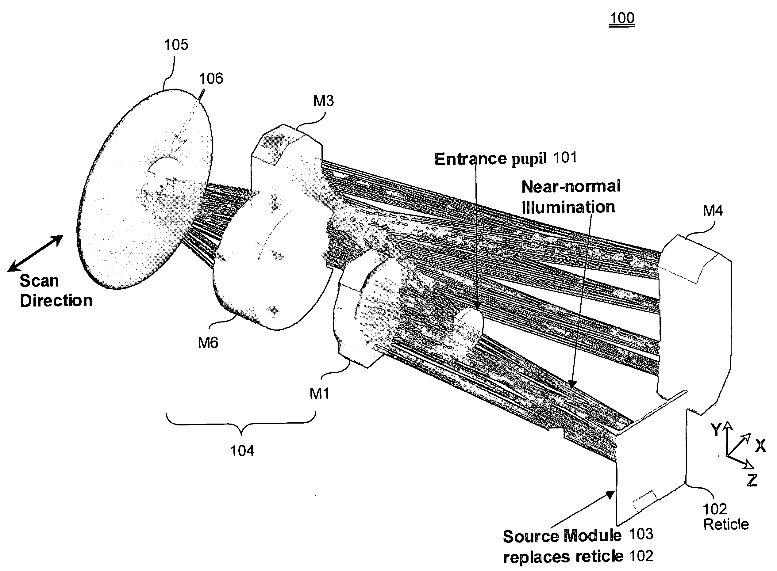
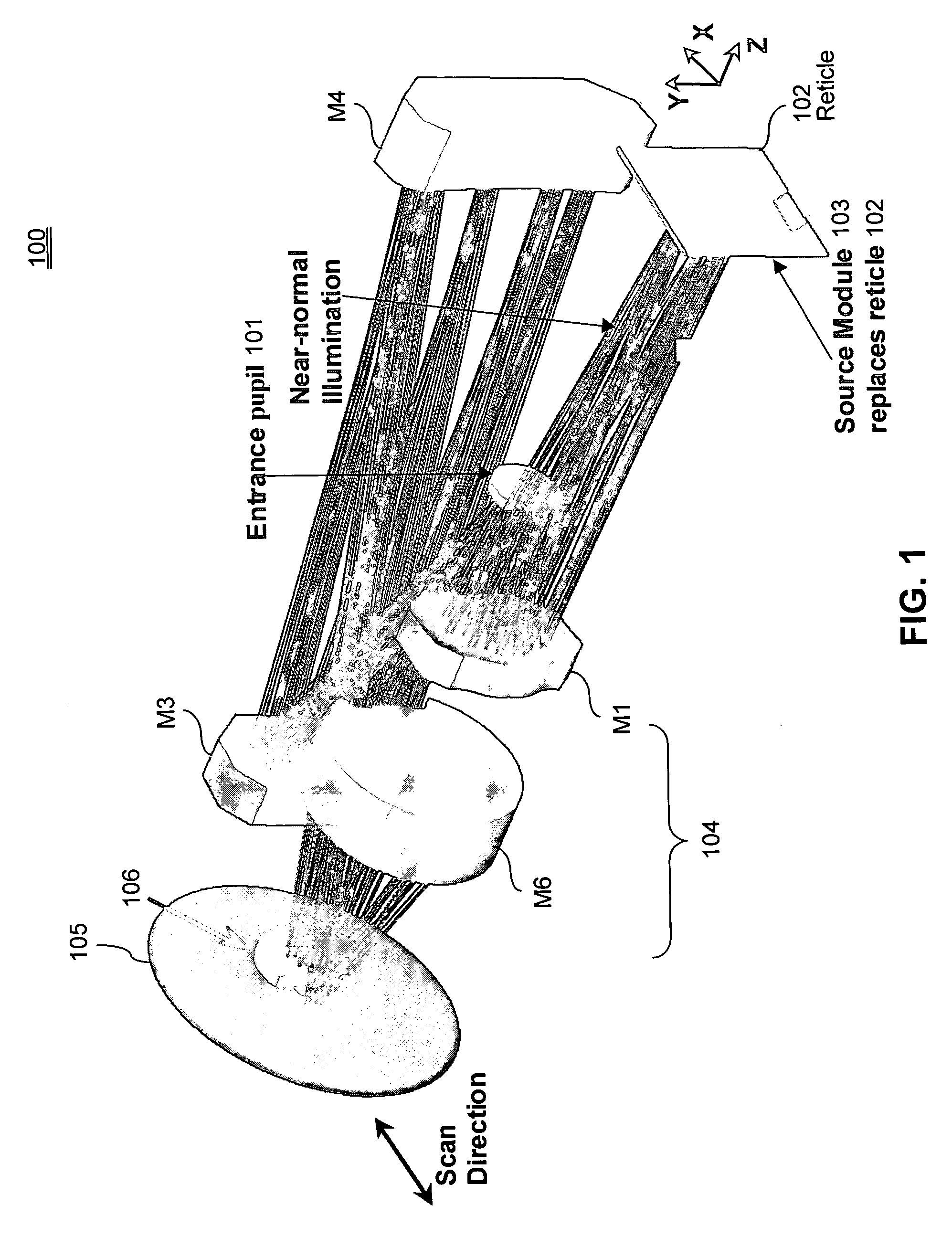
[0025] FIG. 1 illustrates a portion of an EUV photolithographic system 100, which includes an EUV source (not shown in FIG. 1). The system 100 also includes image optics (including mirrors M4 and M3), a pupil 101, a reticle 102 mounted on a reticle stage (RS, not shown) with an image of a pattern to be imaged onto a wafer 105, and projection optics (PO) 104 mirrors M1 and M6. The EUV radiation is then projected onto a wafer 105, which is mounted on a wafer stage (WS, not shown). It will be appreciated that the reticle 102 is reflective in EUV systems, unlike photolithographic systems operating at longer wavelengths, such as deep ultraviolet, or visible, where the reticle 102 is usually transmissive.

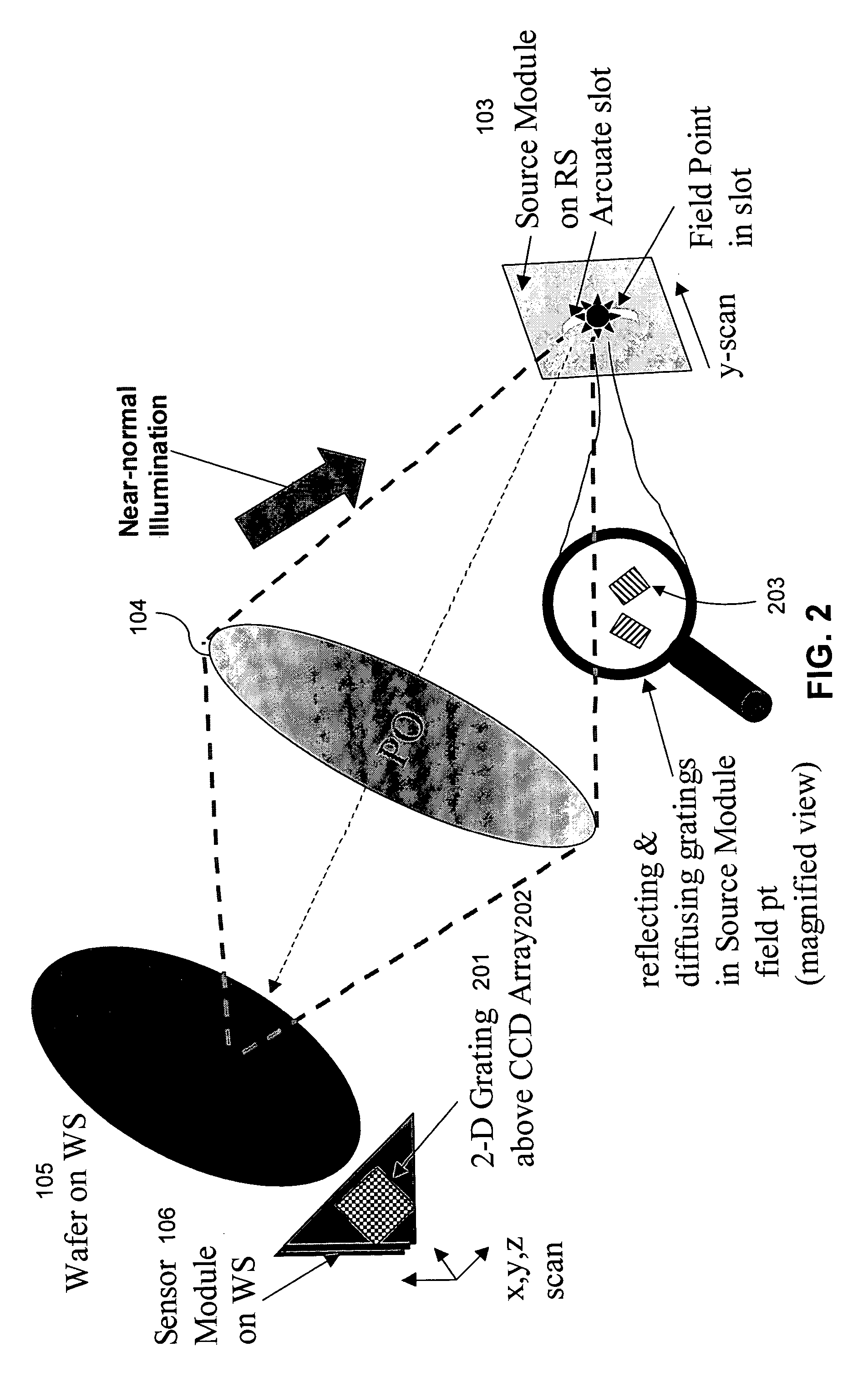
[0026] As further shown in FIG. 1, in the present invention, a sensor module 106 is placed on the wafer stage, and a source module 103 is...


PUM


Abstract

A wavefront measurement system includes a source of electromagnetic radiation. An imaging system directs the electromagnetic radiation at an object plane that it uniformly illuminates. A first grating is positioned in the object plane to condition the radiation entering the input of a projection optic. A projection optical system projects an image of the first grating onto the focal plane. A second grating is positioned at the focal plane that receives a diffracted image of the source to form a shearing interferometer. A CCD detector receives the image of the first grating through the projection optical system and the second grating that forms a fringe pattern if there are aberrations in the projection optical system. Phaseshift readout of fringe pattern can be accomplished by stepping the first grating in a lateral direction and reading each frame with the CCD detector. The first grating includes a plurality of reflecting lines each formed by a plurality of reflecting dots. The first grating has a pitch that is ½ times the magnification of the projection system times the pitch of the second grating for achromatic operation.

Description

[0001] This application claims priority to U.S. Provisional Patent Application No. 60 / 440,051, Filed: Jan. 15, 2003, entitled TAILORED REFLECTING DIFFRACTOR FOR EUV LITHOGRAPHIC SYSTEM ABERRATION MEASUREMENT, which is incorporated by reference herein.[0002] 1. Field of the Invention[0003] The present invention is generally related to extreme ultraviolet (EUV) photolithography systems, and more particularly, to measuring wavefront parameters in a photolithographic system.[0004] 2. Related Art[0005] Lithography is a process used to create features on the surface of substrates. Such substrates can include those used in the manufacture of flat panel displays, circuit boards, various integrated circuits, and the like. A frequently used substrate for such applications is a semiconductor wafer. One skilled in the relevant art would recognize that the description herein would also apply to other types of substrates.[0006] During lithography, a wafer, which is disposed on a wafer stage (WS),...

Claims


Application Information

Patent Timeline
IPC IPC(8): G01J9/02G02B5/18G03F7/20
CPCG01J9/0215G03F7/706G02B5/1838
Inventor POULTNEY, SHERMAN K.
Owner ASML HLDG NV
Why Eureka
Try Eureka