Schottky barrier photodetectors

a technology of photodetectors and barriers, applied in the field of schottky barrier photodetectors, can solve the problems of low external quantum efficiency levels, difficult integration with optical fibers and other optical waveguides in an integrated optical circuit, and inability to achieve uniform absorption over a wavelength rang

Inactive Publication Date: 2004-09-09
UNIVERSITY OF OTTAWA
View PDF15 Cites 23 Cited by
  • Summary
  • Abstract
  • Description
  • Claims
  • Application Information

AI Technical Summary

Benefits of technology

0009] An object of the present invention is to overcome or at least mitigate the disadvantages of the prior art photodetectors, or at least provide an alternative.

Problems solved by technology

Normally incident light passes through the Schottky barrier once, which only absorbs a portion of the light leading to low external quantum efficiency levels.
However, the absorption will not be uniform over a wavelength range, as has been noted by Elabd and Kosonocky in "Theory and Measurements of Photoresponse for Thin Film PdSi and PtSi Infrared Schottky-Barrier Detectors With Optical Cavity," RCA Review 43, pp.
All of the above mentioned prior art require that the incident light be either normal or at a specific angle to the metal-semiconductor interface, making integration with optical fibers and other optical waveguides in an integrated optical circuit difficult.
This is still not entirely satisfactory since at least 30% of the incident light is lost.

Method used


Image

  • Schottky barrier photodetectors
  • Schottky barrier photodetectors
  • Schottky barrier photodetectors

Examples


Embodiment Construction

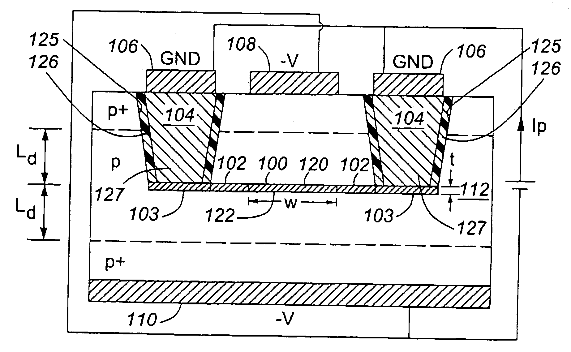
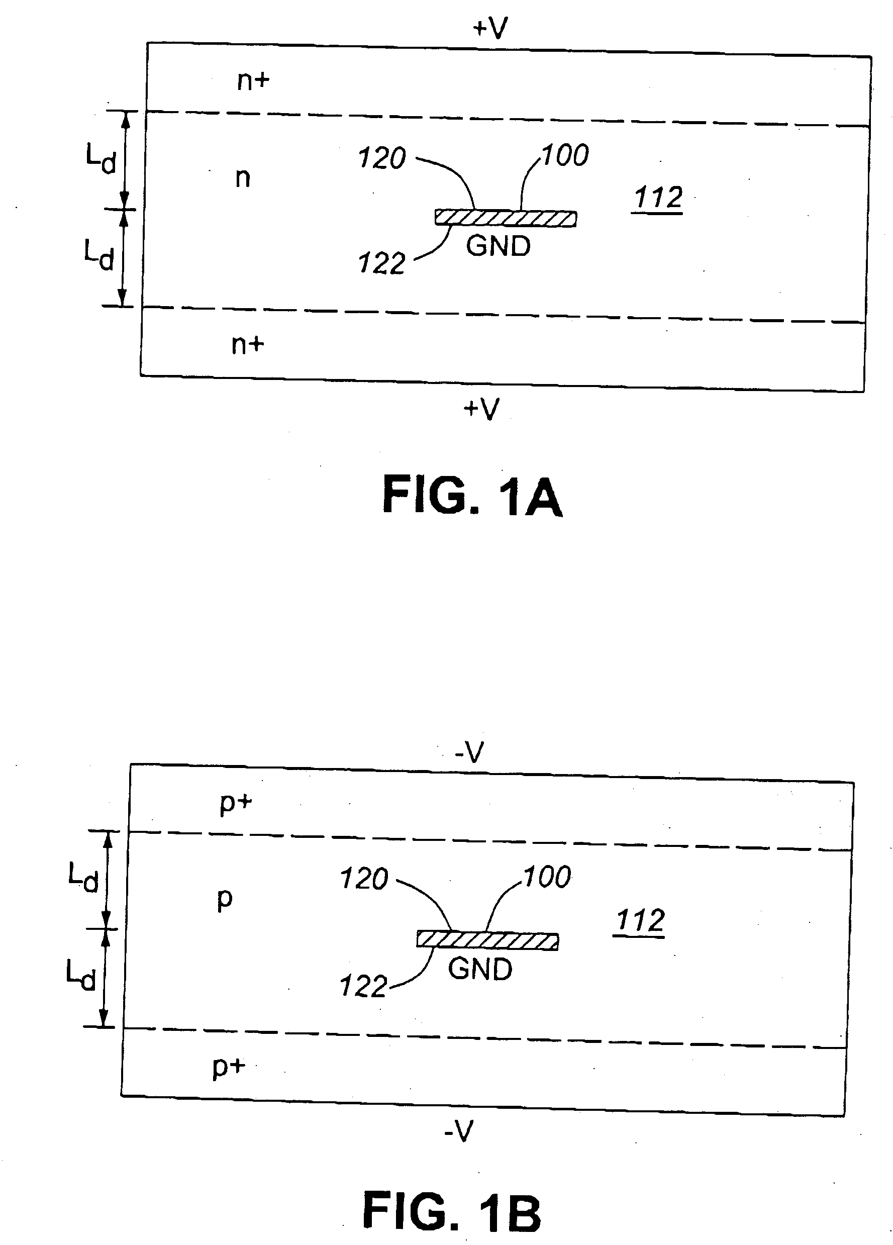
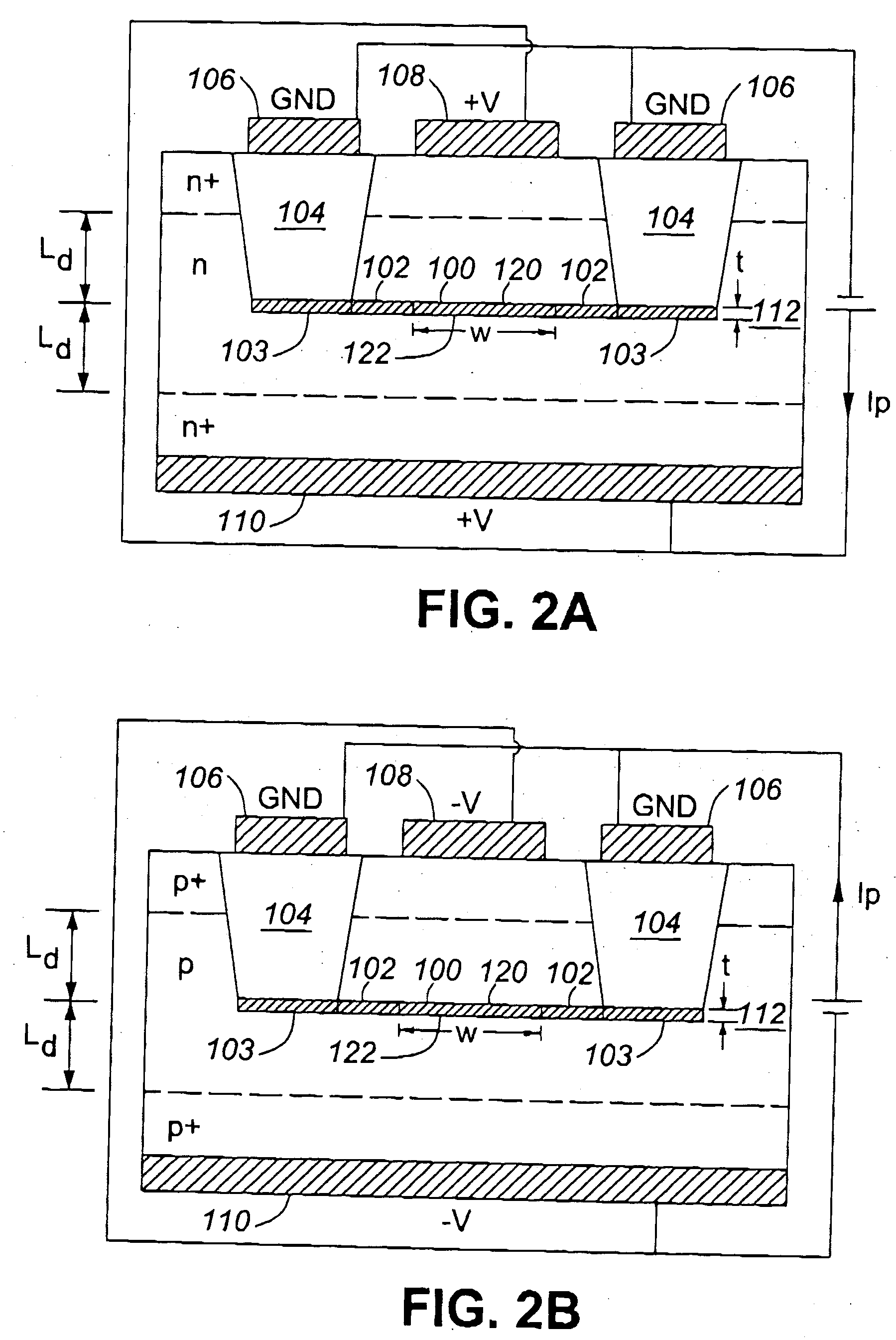
[0083] From the theory developed above, it is clear that both the Schottky barrier height and the Schottky barrier / waveguide dimensions affect the photodetector performance. The length and cross sectional area of the waveguide affect the absorption; the longer, wider and thicker the waveguide the greater the absorption of light in the metal layer. The surface area of the Schottky barrier contact affects the dark current of the detector; the larger the metal-semiconductor contact area the greater the dark current. The greater the dark current the higher the minimum detectable power. Just as the waveguide dimensions have conflicting effects on the photodetector performance so does the Schottky barrier height. The lower the Schottky barrier, the higher the dark current and minimum detectable power but the higher the responsivity, as well. The absorption of the metal waveguide depends not only on the dimensions of the waveguide but also on the material selection. Depending on the optica...


PUM


Abstract

A Schottky barrier photodetector comprises a waveguide structure formed by a thin strip of material having a relatively high free charge carrier density, for example a conductor or certain classes of highly-doped semiconductor, surrounded by material having a relatively low free charge carrier density, the material on at least one side of the strip comprising a semiconductor, the strip having finite width and thickness with dimensions such that optical radiation couples to the strip and propagates along the length of the strip as a plasmon-polariton wave, light for detection being coupled to one end of the strip to propagate along the strip as said plasmon-polariton wave, ohmic contact means applied to the semiconductor material and at least one electrode means connected to the strip for applying bias to the Schottky barrier and extracting a photodetector current corresponding to the light applied to the photodetector. Where the strip of material is a flat, thin strip, the device will be polarisation dependent. Substantially polarisation-independent operation maybe achieved by using a strip whose width is of the same order as its thickness.

Description

[0001] This application claims priority from U.S. Provisional application No. 60 / 451,257 filed Mar. 4, 2003, the contents of which are incorporated herein by reference.[0002] The invention relates generally to photodetectors, and more particularly to Schottky barrier photodetectors.[0003] Semiconductor devices using metal-semiconductor barriers, known as Schottky barriers, instead of p / n junctions, have been developed to convert incident light into electrical energy. Silicon is often used as the semiconductor in Schottky barrier photodetectors for detecting in the infrared portion of the electromagnetic spectrum. Schottky barrier infrared photodetectors are well known in the art.[0004] Examples of prior art Schottky barrier infrared photodetectors are disclosed in U.S. Pat. No. 4,531,055 to Shepperd Jr. et al and in U.S. Pat. No. 4,533,933 to Pellegrini et al. These prior art examples are planar devices in which the Schottky barrier photodetectors are comprised of a thin metal film,...

Claims


Application Information

Patent Timeline
Patent Type & Authority Applications(United States)
IPC IPC(8): H01L31/108
CPCH01L31/1085H01L31/108
Inventor SCALES, CHRISTINE ANNBERINI, PIERRE SIMON JOSEPH
Owner UNIVERSITY OF OTTAWA
Why Eureka
Try Eureka