
Laminated radiation detector and process for fabrication thereof

a technology of laser radiation detector and fabrication process, which is applied in the direction of radiation measurement, instruments, measurement devices, etc., can solve the problems of limited size, high cost and time consumption, and current flowing between the electrodes, and achieves high tolerances and enhance product robustness

Inactive Publication Date: 2004-10-07
REAL TIME RADIOGRAPHY
View PDF13 Cites 6 Cited by
  • Summary
  • Abstract
  • Description
  • Claims
  • Application Information

AI Technical Summary

Benefits of technology

[0027] It is a further object of the present invention embodiments to provide a means of producing coating layers to higher tolerances.
[0105] By constructing continuous multi-layer planar structures for applying to pixilated substrates to form detector and imager devices, whereby the multi-layer planar structures may be subjected to rigorous inspection before they are applied to the pixilated substrates, significant savings may result. Furthermore, the procedure produces cost saving by reducing the number of improperly fabricated pixelated substrates.

Problems solved by technology

Bombardment by high-energy photons, such as X-rays and gamma rays, results in the formation of hole-electron pairs, which causes current to flow between the electrodes.
These are, however, expensive and time consuming to grow, and only limited sizes have been achieved.
Despite the above mentioned and other advantages of HgI.sub.2 for high energy radiation detectors and imagers, HgI.sub.2 has the disadvantage that the material is corrosive, and is not compatible with aluminum and copper bus lines and the like, often used for TFT electronics in preferred substrates.
This problem is exacerbated by the traditional wet manufacturing processes used, whereby adhesives comprising large quantities of organic solvents are used for adhering detectors, cut from single crystal wafers, to the substrate.
A further disadvantage of the current state of the art is that coatings are applied to commercially acquired and rather expensive pixilated substrates.
If the coated substrates prove unacceptable, there is little choice but to discard the coated substrate, as cleaning off the coating, leaving a useable substrate is usually impractical.
In addition, there is an inherent difficulty in the application of liquid coatings to pixilated glass substrates in that currently available pixilated glass substrates have raised pixels and a topography that varies by anything from 1-7 microns from pixel to pixel.
This poor tolerance adversely affects the desired thickness uniformity of the dried layer.
Currently available pixilated substrates are fabricated from glasses and ceramics, and these stiff substrates cannot be flexed to position them precisely with respect to the applicator.
It is inherently undesirable to deposit coating layers on pixilated substrates through coating and drying operations, since such handling operations subject the pixilated substrates to temperature, chemical and physical stresses, and since pixilated substrates, the most expensive elements of the detector, can be easily damaged.

Method used


Image

  • Laminated radiation detector and process for fabrication thereof
  • Laminated radiation detector and process for fabrication thereof
  • Laminated radiation detector and process for fabrication thereof

Examples


Embodiment Construction

[0103] Referring now to FIG. 6, a cross-sectional schematic of a multi-layer prototype structure 410 is shown. As shown in FIG. 6, a multi-layer prototype structure 410 comprising a commercially available PET film 420 coated with an ITO layer 430 was adhered to a 200 micron thick HgI.sub.2 and polystyrene composite layer 450, using a 160 micron thick double sided adhesive film 440 available from SPI Supplies, West Chester, Pa., Adhesive Research Inc., Glen Rock, Pa. or 3M, Minneappolis, Minn., among others. The multi-layer structure was adhered to an ITO 460 glass substrate 480 using one 1 cm.times.1 cm `pixel` of double-sided conductive film 470. Areas 465 represent voids between ITO 460 glass substrate 480 and HgI.sub.2 and polystyrene composite layer 450.

[0104] FIGS. 7, 8 and 9 are graphs showing the sensitivity, dark current and sensitivity to dark current ratio responses, respectively, with respect to applied bias for the prototype in FIG. 6. The results obtained demonstrate th...


PUM


Abstract

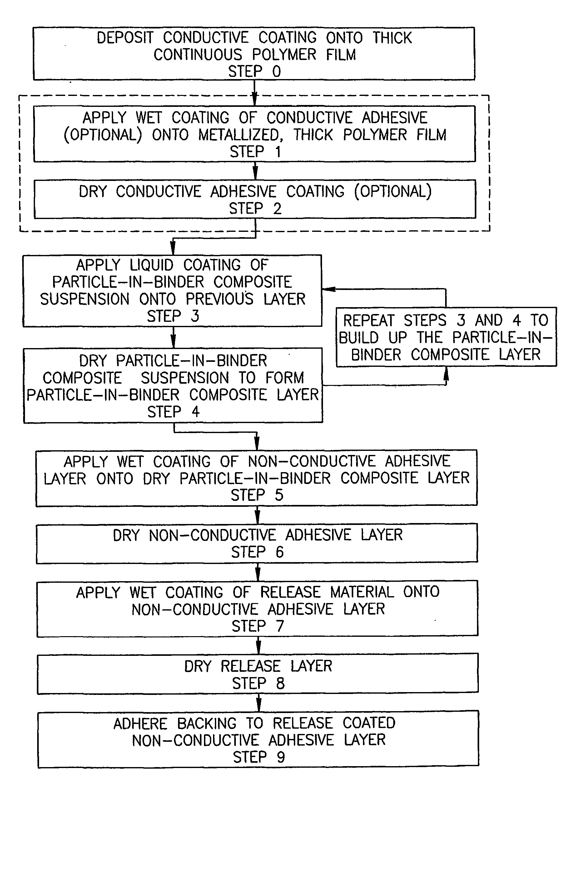
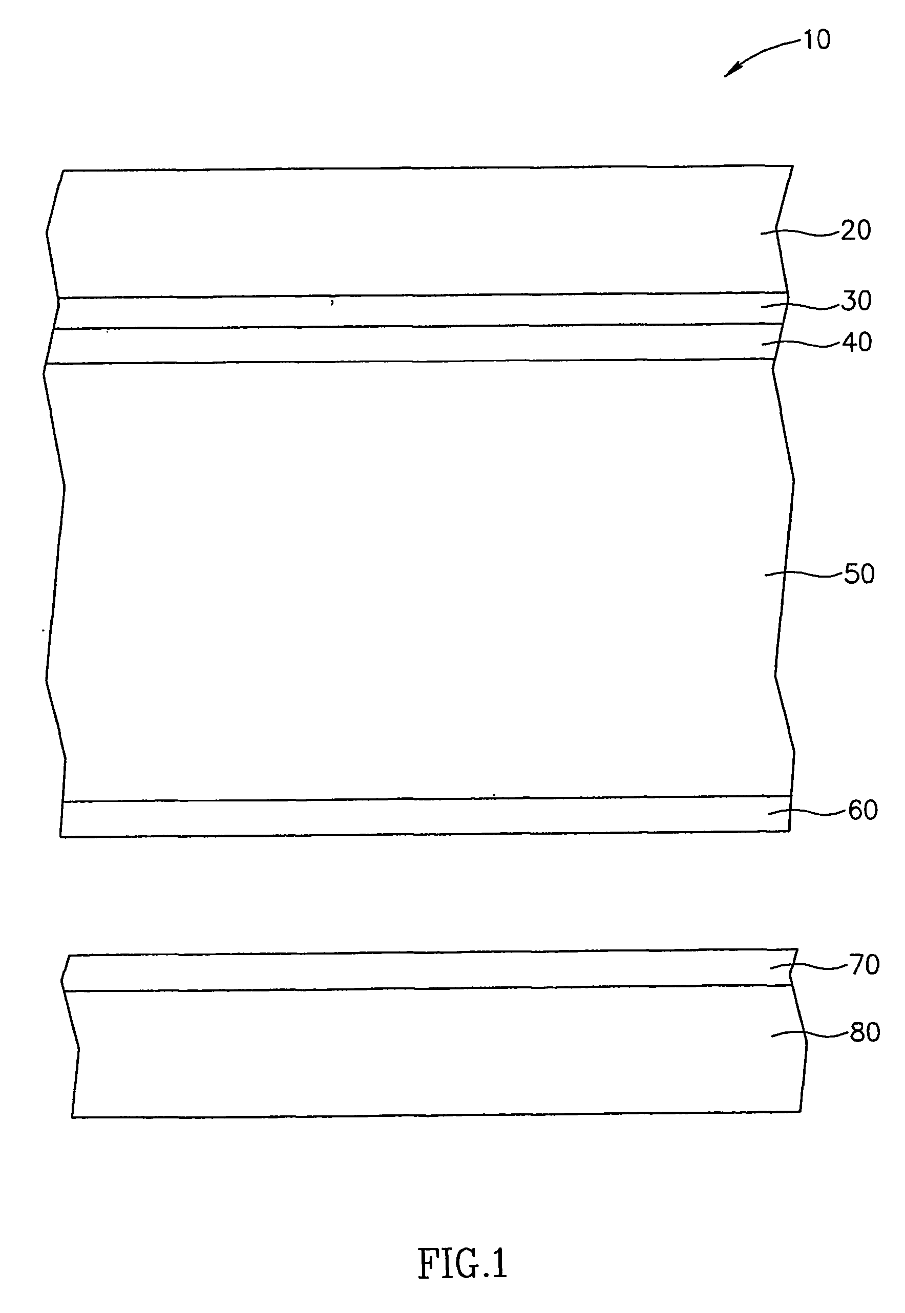
A continuous multi-layer construction for detecting radiation including a polymer layer, a conducting electrode layer affixed to the polymer layer and a particle-in-binder composite layer affixed to the conducting electrode layer, where the composite layer absorbs photons. A process for fabricating continuous multi-layer constructions for detection of radiation including the following steps: depositing a conducting electrode layer onto a polymer film, applying at least one coating layer of a particle-in-binder composite onto the conducting electrode layer, and drying the at least one coating layer of the particle-in-binder composite.

Description

[0001] The present invention relates to large area multi-layer polymer based high energy electromagnetic radiation detecting and imaging devices, systems containing such devices, and processes for the fabrication thereof.[0002] X-ray and gamma ray detection are useful in a wide variety of scientific and technical endeavors. These include medical imaging applications such as X-ray radiography, X-ray computed tomography (CT), single photon emission computed tomography (SPECT) and positron emission tomography (PET). Also of note are non-destructive testing and quality control of manufacturing components, baggage inspection systems, such as those installed at customs, and astrophysics and astronomy applications, such as galactic surveys and space exploration.[0003] Special photographic plates can be used for X-ray detection. For repeated use however, and for maximum data collection, semiconductor detectors exhibiting the well known photo-electric effect, whereby incident photons of radi...

Claims


Application Information

Patent Timeline
IPC IPC(8): G01TG01T1/24G01T1/29
CPCG01T1/2928
Inventor WHEELER, JAMES MREISMAN, BENJAMIN JOSHUASCHIEBER, MICHAELHERMON, HAIMSHTEKEL, ELIEZERMELEKHOV, LEONID
Owner REAL TIME RADIOGRAPHY
Learn More