Magnetoresistance effect element, magnetic head, and magnetic reproducing apparatus

Active Publication Date: 2004-10-14
KK TOSHIBA
View PDF5 Cites 106 Cited by
  • Summary
  • Abstract
  • Description
  • Claims
  • Application Information

AI Technical Summary

Benefits of technology

0247] In the above, the first through fourth embodiments of the invention have been explained. The magneto

Problems solved by technology

However, as mentioned above, it is necessary to laminate magnetic layers and non-magnetic layers repeatedly by turns in order to earn resistance in the case of the CPP type MR element, therefore, it is technically very difficult to individually control the magnetization of each of such many the magnetic layers.
However, since the number of pinned layers and free layers becomes m

Method used


Image

  • Magnetoresistance effect element, magnetic head, and magnetic reproducing apparatus
  • Magnetoresistance effect element, magnetic head, and magnetic reproducing apparatus
  • Magnetoresistance effect element, magnetic head, and magnetic reproducing apparatus

Examples


second example

[0275] Next, the magnetoresistance effect elements using the spinodal decomposition of aluminum (Al)-gold (Au) system will be explained as the second example of the invention.

[0276] Also in this example, the magnetoresistance effect elements shown in FIG. 1 were fabricated. However, the magnetically pinned layer 4 was made into the so-called "synthetic structure" in this example.

[0277] Moreover, the manufacturing method of this example is almost the same as that mentioned above about the first example. However, the phase separation layer 9 was formed, irradiating the ion beam containing oxygen ion on a substrate simultaneously with films formation.

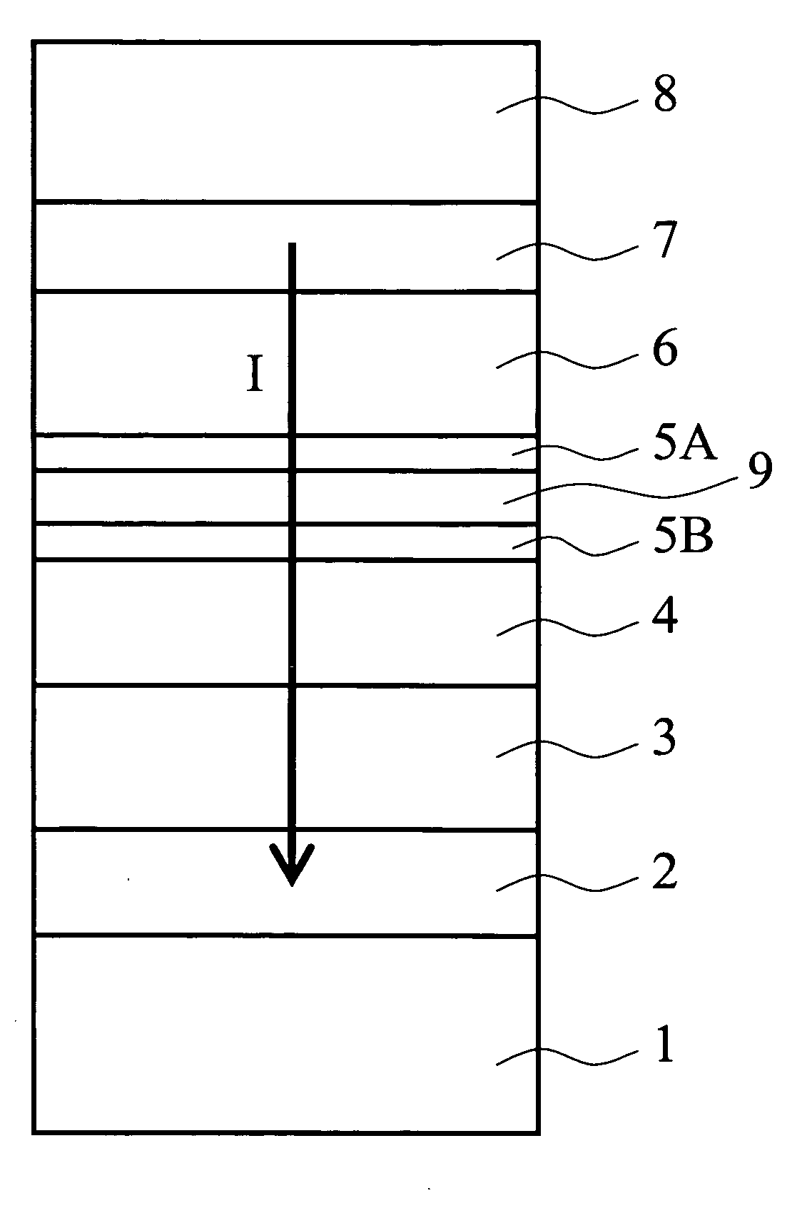
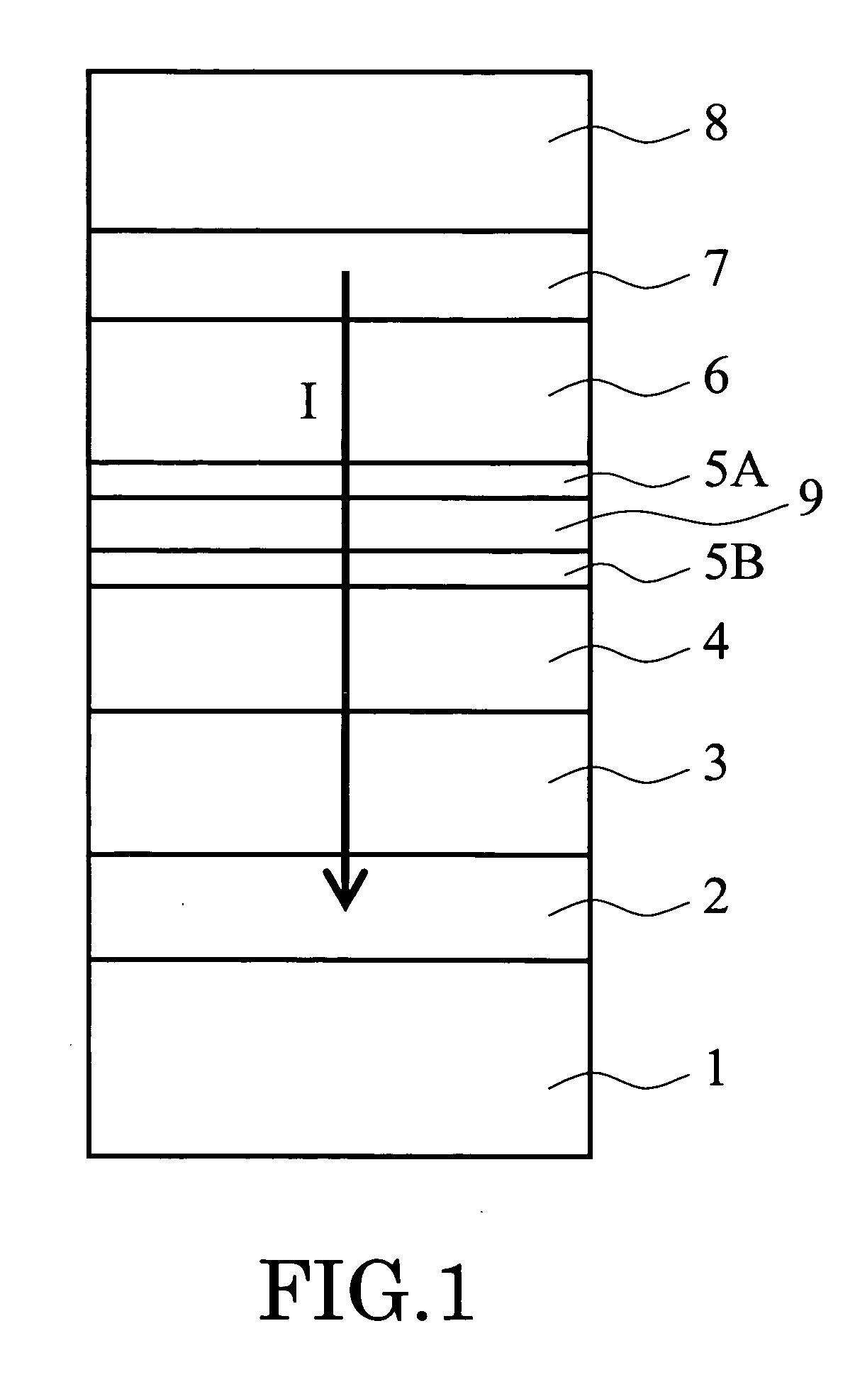
[0278] The thickness and material of each layer which constitutes the magnetoresistance effect element are as the following:

[0279] Si substrate (1) / 5 nm Ta (2) / 200 nm Cu (2) / 5 nm (Ni.sub.80Fe.sub.20).sub.8Cr.sub.22 (2) / 10 nm PtMn (3) / 2.5 nm CoFe(4) / 0.9 nm Ru (4) / 2.5 nm CoFe (4) / 0.2 nm Cu (5A) / 0.8 nm AlAu (9) / 0.2 nm Cu (5B) / 3 nm CoFe (6) / 2 ...

third example

[0290] Next, the magnetoresistance effect elements using the spinodal decomposition of copper (Cu)-nickel (Ni)-iron (Fe) system will be explained as the third example of the invention.

[0291] Also in this example, the magnetoresistance effect elements shown in FIG. 1 were fabricated. However, the interface adjusting layer 5B was not provided, and the magnetically pinned layer 4 was made into the so-called "synthetic structure" in this example.

[0292] The thickness and material of each layer which constitutes the magnetoresistance effect element are as the following:

[0293] Si substrate (1) / 5 nm Ta (2) / 200 nm Cu (2) / 5 nm (Ni.sub.80Fe.sub.20).sub.78Cr.sub.22 (2) / 10 nm PtMn (3) / 2.5 nm CoFe (4) / 0.9 nm Ru (4) / 2.5 nm CoFe (4) / 0.8 nm CuNiFe (9) / 2.0 nm Cu (5) / 3 nm CoFe (6) / 2 nm Ta (7) / 200 nm Cu (8).

[0294] In the above, the reference numerals expressed in FIG. 1 are given to the each corresponding layer with parenthesis.

[0295] CuNiFe alloy used for the base material of the phase separation laye...

fourth example

[0307] Next, the magnetoresistance effect element which comprises two phase separation layers will be explained as a fourth example of the invention.

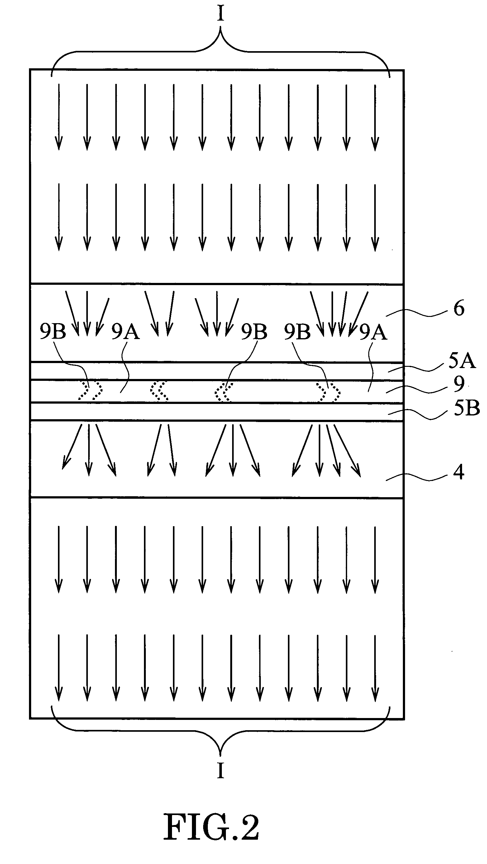
[0308] FIGS. 17 and 18 are schematic diagrams showing the cross-sectional structure of the magnetoresistance effect elements of this example. The same reference numerals are given to the same elements as what were mentioned above about FIG. 1 through FIG. 16 also about these figures, and detailed explanation is omitted.

[0309] That is, in the structure of FIG. 17, the phase separation layer 9 is inserted not only the portion of a spacer layer but in the magnetization pinned layer 4. Moreover, in the structure of FIG. 18, the phase separation layer 9 is inserted not only the portion of a spacer layer but in the magnetization free layer 6.

[0310] The magnetoresistance effect elements of this example were fabricated by the methods almost same as the method mentioned above about the first example.

[0311] The thickness and material of each laye...


PUM


Abstract

A magnetoresistance effect element comprises: a magnetoresistance effect film, a pair of electrodes, and a phase separation layer. The magnetoresistance effect film includes a first ferromagnetic layer whose direction of magnetization is pinned substantially in one direction, a second ferromagnetic layer whose direction of magnetization changes in response to an external magnetic field, and an intermediate layer provided between the first and second ferromagnetic layers. The pair of electrodes are electrically coupled to the magnetoresistance effect film and configured to supply a sense current perpendicularly to a film plane of the magnetoresistance effect film. The phase separation layer is provided between the pair of electrodes. The phase separation layer has a first phase and a second phase formed by a phase separation in a solid phase from an alloy including a plurality of elements. One of the first and second phases includes at least one element selected from the group consisting of oxygen, nitrogen, fluorine and carbon in higher concentration than other of the first and second phases.

Description

[0001] This application is based upon and claims the benefit of priority from the prior Japanese Patent Application No. 2002-265883, filed on Sep. 11, 2002; the entire contents of which are incorporated herein by reference.[0002] The present invention relates to a magnetoresistance effect element, a manufacturing method of a magnetoresistance effect element, a magnetic head and a magnetic reproduction apparatus, and more particularly, it relates to a magnetoresistance effect element where a sense current flows perpendicularly to the film plane, a manufacturing method of the magnetoresistance effect element, and a magnetic head and a magnetic reproduction apparatus including the magnetoresistance effect element.[0003] Although a magnetic storage density of HDD (hard disk drive) is improved dramatically in recent years, it has been desired to raise the magnetic storage density further. Since a record bit size becomes small as the magnetic storage density is raised, a reproducing sensi...

Claims


Application Information

Patent Timeline
IPC IPC(8): G11B5/39
CPCG11B5/3906Y10T428/1121H01L43/12H01L43/08H10N50/01H10N50/10
Inventor HASHIMOTO, SUSUMUKOUI, KATSUHIKOSAHASHI, MASASHIIWASAKI, HITOSHI
Owner KK TOSHIBA
Why Eureka
Try Eureka