Optical module and method of manufacturing the same, and hybrid integrated circuit, hybrid circuit board, electronic apparatus, opto-electricity mixed device, and method of manufacturing the same

a technology of optical modules and manufacturing methods, applied in the field of optical modules, can solve the problems of high power consumption and the like, noise radiation, cross talk between signal lines,

Inactive Publication Date: 2004-11-25
SEIKO EPSON CORP
View PDF2 Cites 113 Cited by
  • Summary
  • Abstract
  • Description
  • Claims
  • Application Information

AI Technical Summary

Benefits of technology

[0009] Thus, after having arranged the jig which has the protruding portion, for example, above the transparent substrate, the position of the jig is fine-adjusted according to the configuration of the electro-optical element, and then the filler material is cured to narrow the inner side of the guide hole after the fine adjustment, thereby enabling to form the guide hole with increasing the precision of the formation position, the size and the like. By inserting the guide pin into the guide hole, the mutual positioning of the transparent substrate and optical transmission line support member can be aligned with high precision. Therefore, enhancement of the optical coupling efficiency can be attained by aligning and arranging precisely and easily the mutual positions of the optical transmission line and the electro-optical element. Moreover, what is required for the size of the guide hole is a size, which is sufficient to adjust a position of the protruding portion provided to the jig. Thus there is another advantage that the formation becomes easy because the required precision for the formation position and the hole diameter decreases.
[0038] This configuration enables precise and easy alignment of the mutual positions of the optical transmission line and the hybrid integrated circuit chip, which the circuit board has, and thus enhancement of the optical coupling efficiency can be attained. Especially, what is required for the size of the guide hole is a size, which is sufficient to adjust a position of the protruding portion provided to the jig or the guide pin, and thus there is another advantage that the formation becomes easy because the required precision for the formation position and the hole diameter decreases.

Problems solved by technology

Acceleration of a signal transfer rate between circuit chips or between circuit boards and the like included in various apparatus has advanced, and thus problems of cross talk between signal lines, noise radiation, impedance mismatching, high power consumption and the like are becoming critical.

Method used


Image

  • Optical module and method of manufacturing the same, and hybrid integrated circuit, hybrid circuit board, electronic apparatus, opto-electricity mixed device, and method of manufacturing the same
  • Optical module and method of manufacturing the same, and hybrid integrated circuit, hybrid circuit board, electronic apparatus, opto-electricity mixed device, and method of manufacturing the same
  • Optical module and method of manufacturing the same, and hybrid integrated circuit, hybrid circuit board, electronic apparatus, opto-electricity mixed device, and method of manufacturing the same

Examples


first exemplary embodiment

[0051] (First Exemplary Embodiment)

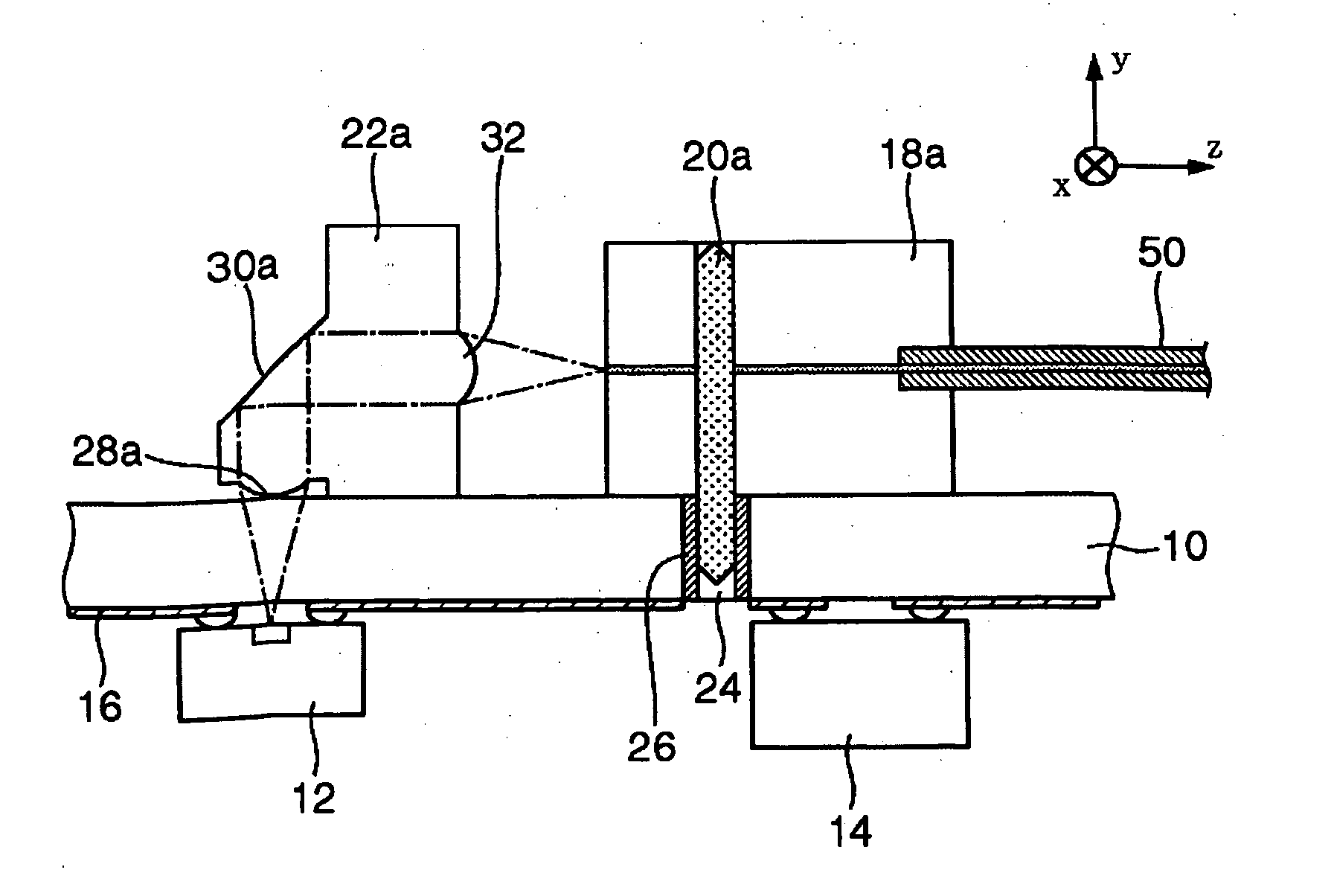
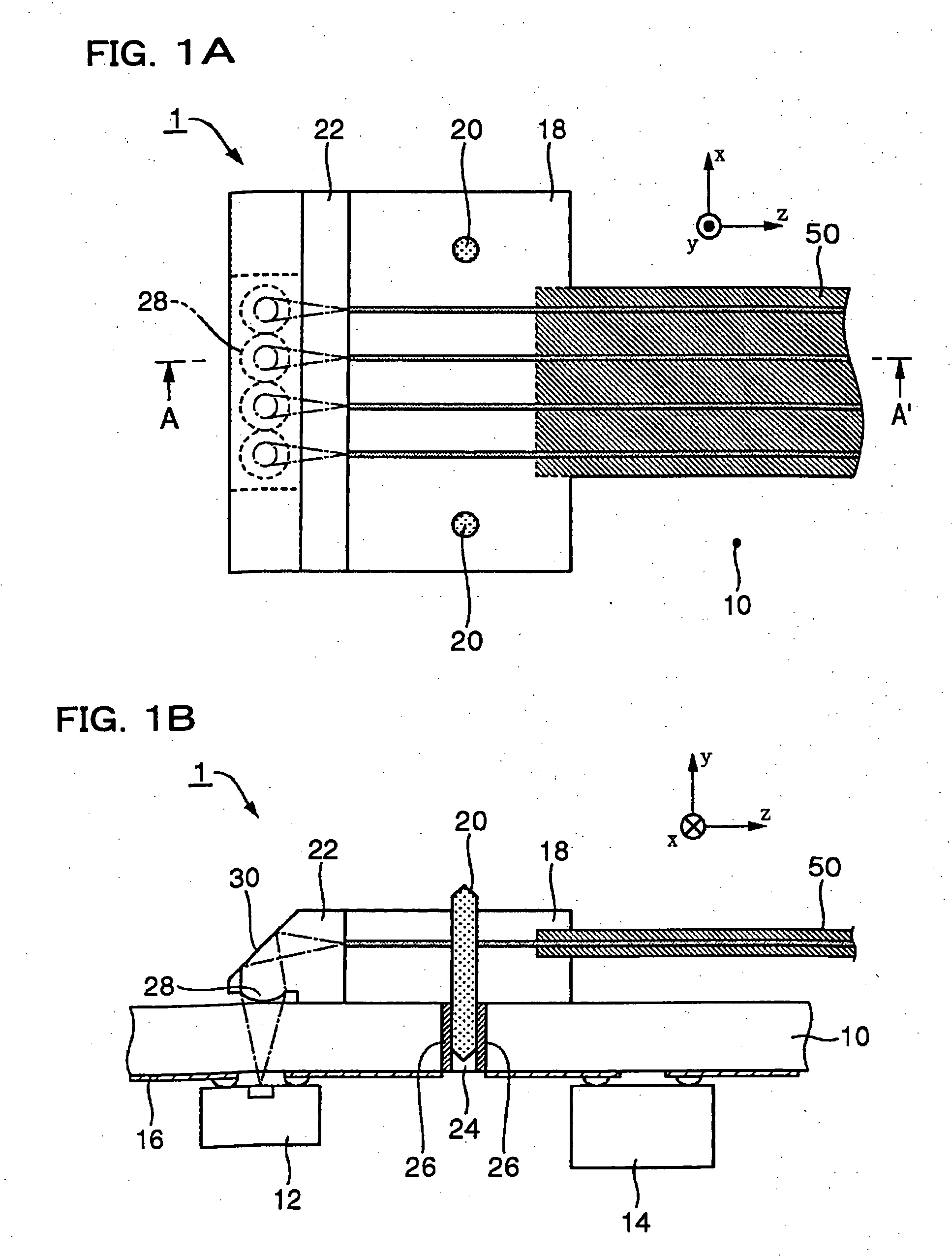
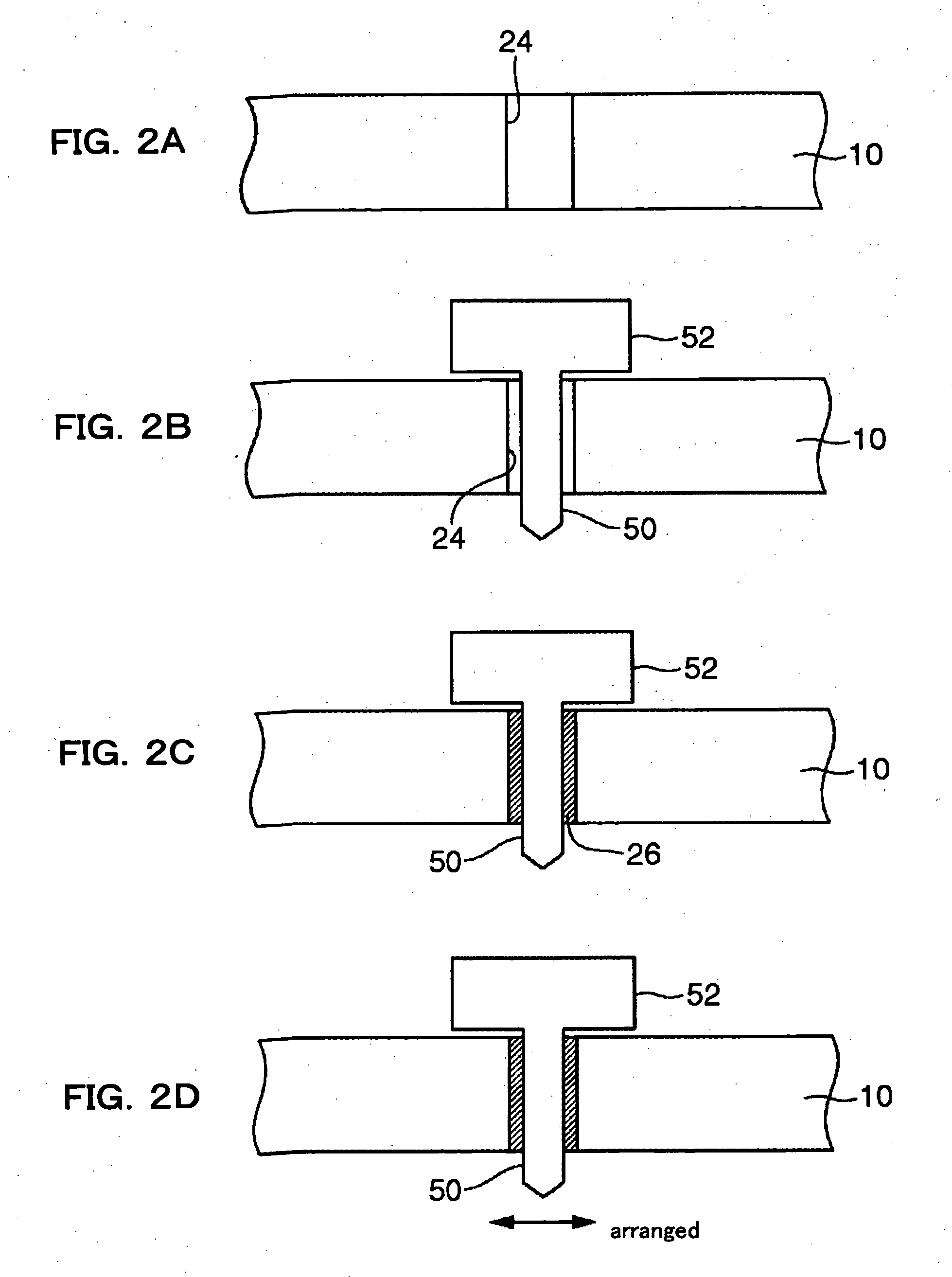
[0052] FIG. 1 is a view explaining a configuration of an optical module (opto-electric transmission line conversion connector) of the exemplary embodiment. FIG. 1(A) shows a plan view of the optical module of the exemplary embodiment. FIG. 1(B) shows a sectional view taken along the A-A' plane of FIG. 1(A). In addition, in FIG. 1(B), in order to describe a structure of a guide pin 20 (described hereinafter in detail) and its vicinity, such a region is shown by replacing the sectional view taken along the A-A' plane.

[0053] The optical module 1 shown in FIG. 1 includes a transparent substrate 10, an electro-optical element 12, an electronic circuit 14, a wiring film 16, a fiber support member 18, a guide pin 20, and an optical coupling member 22.

[0054] The transparent substrate 10 has optical permeability to the wavelength of the light used, and supports each element, which constitutes the optical nodule 1. For example, in a case that the wavelength ...

second exemplary embodiment

[0084] (Second Exemplary Embodiment)

[0085] Next, a hybrid integrated circuit (opto-electricity mixed integrated circuit) constituted using the optical module in the above described exemplary embodiment, and a hybrid circuit board constituted using the hybrid integrated circuit will be described.

[0086] FIG. 6 is a view explaining an exemplary embodiment of a configuration of a hybrid integrated circuit and a hybrid circuit board including the hybrid integrated circuit. A hybrid circuit board 200 shown in this view includes a hybrid integrated circuit 100 including the optical module 1 (or 1a, 1b) according to the exemplary embodiments described above, and a wiring board 108.

[0087] The hybrid integrated circuit 100 includes the optical module 1 and a signal-processing chip 102, and has a structure which moulds and integrates both with plastic and the like. The optical module 1 and the signal-processing chip 102 are coupled electrically by wire bonding. The optical module 1 is arranged...

third exemplary embodiment

[0090] (Third Exemplary Embodiment)

[0091] Next, an opto-electricity mixed device, which has a structure similar to the hybrid circuit board according to the above-described second exemplary embodiment, will be described.

[0092] FIG. 8 is a view explaining a configuration of an opto-electricity mixed device 300 according to a third exemplary embodiment. An opto-electricity mixed device 300 shown in this view includes a hybrid integrated circuit chip 120 and a circuit board 126.

[0093] The hybrid integrated circuit 120 includes an optical module 121 and a signal-processing chip 122, and has a structure which moulds and integrates the both with plastic and the like. The optical module 121 and the signal-processing chip 122 are coupled electrically by wire bonding. The optical module 121 has a structure which excludes the fiber supporting member 18 and the optical coupling member 22 from the optical module 1 (refer to FIG. 1) in the above-described exemplary embodiment, and is arranged so...


PUM


Abstract

To provide a technology, which enable carrying out an optical position alignment precisely and easily in apparatus and the like used in optical communication, a method of manufacturing an optical module includes forming a guide pin in either a transparent substrate or an optical transmission line support member; forming a guide hole, in which the guide pin is to be inserted, to the other one of the transparent substrate and the optical transmission line support member such that the diameter of the guide hole is made larger as compared with the diameter of the hole; arranging a jig having a protruding portion, of which diameter is substantially the same as the diameter of the guide pin, over the transparent substrate such that the protruding portion is being inserted into the guide hole; filling the gap between the protruding portion and the guide hole with a filler material, which is cured by carrying out a predetermined processing; adjusting a position of the jig; curing the filler material, which is filled in the gap between the protruding portion and the guide pin; and pulling out the protruding portion from the guide hole.

Description

[0001] 1. Field of Invention[0002] The present invention relates to apparatus, components and the like, which carry out information communication (signal transmission) between a plurality of apparatus or within an apparatus and the like, by using an optical signal.[0003] 2. Description of Related Art[0004] Acceleration of a signal transfer rate between circuit chips or between circuit boards and the like included in various apparatus has advanced, and thus problems of cross talk between signal lines, noise radiation, impedance mismatching, high power consumption and the like are becoming critical. For this reason, optical communication is beginning to be introduced even for signal transmission inside an apparatus. Furthermore, a method of transmitting an optical signal through an optical fiber (tape fiber) or an optical waveguide, instead of other methods of running electric signal in metal wiring, between circuit chips and between modules and the like inside an apparatus, is being ...

Claims


Application Information

Patent Timeline
Patent Type & Authority Applications(United States)
IPC IPC(8): G02B6/122G02B6/42H05K1/02
CPCG02B6/4214G02B6/4231G02B6/4249
Inventor NAGASAKA, KIMIOMIYAMAE, AKIRAKANEKO, TAKEO
Owner SEIKO EPSON CORP
Why Eureka
Try Eureka