Display device and manufacturing method thereof

a technology of a display device and a manufacturing method, applied in the direction of semiconductor devices, basic electric elements, electrical apparatus, etc., can solve the problems of indium tin oxide not crystallizing, crystalline components remaining as residues after wet etching, and amorphous

Active Publication Date: 2004-12-02
SEMICON ENERGY LAB CO LTD
View PDF10 Cites 39 Cited by
  • Summary
  • Abstract
  • Description
  • Claims
  • Application Information

AI Technical Summary

Benefits of technology

[0015] In particular, indium tin oxide (ITO) containing one or both of silicon oxide (SiO.sub.2) and silicon (Si) is completely amorphous without a crystalline component mixed in during deposition, and no residue is generated when a weak acid solution such as oxalic acid is used for etching the indium tin oxide, so that etching can be performed easily. In addition, the indium tin oxide is not crystallized at least by heat treatment of 250.degree. C. or less, and remains amorphous. Furthermore, since the indium tin oxide has few projections generate to be highly flat and smooth, it is also an advantage that a polishing process after forming the second transparent conductive film becomes easier. The indium tin oxide (ITO) containing one or both of silicon oxide (SiO.sub.2) and silicon (Si) can be formed by sputtering with indium tin oxide containing silicon oxide (SiO.sub.2) from 1 to 10 wt % as a target.
[0019] As the conductive film that has a low resistance of a specific resistance of 3 .mu..OMEGA. or less, metal such as aluminum (Al) and copper (Cu) can be used. By covering the conductive film with the first and second transparent conductive films, oxidation of the conductive film can be prevented and the specific resistance can be prevented from increasing.
[0021] A residue caused by etching a film of amorphous indium tin oxide is likely to be generated particularly on a silicon nitride film formed by sputtering. However, in a display device that has a light-emitting element, it is preferable to provide a silicon nitride film formed by sputtering below the light-emitting element in order to prevent an impurity from being mixed into a TFT from the light-emitting element. In addition, in the case of using a flexible organic resin film such as acrylic or polyimide as an interlayer insulating film, polishing becomes easier in a polishing process after forming the second transparent conductive film when a structure that has a rigid inorganic film such as a silicon nitride film below the first transparent conductive film is employed. Accordingly, the present invention is effective also in the case of forming an electrode including a transparent conductive film on a silicon nitride film formed by sputtering.
[0022] In the present invention, in the case of using crystalline indium tin oxide as the second transparent conductive film, it is an advantage that metals included in a solution for polishing such as iron (Fe) and potassium (K) can be removed with the use of a strong acid solution when chemical mechanical polishing (CMP) is used to perform a polishing process for removing a projection at a surface of the second transparent conductive film. In this case, it is preferable to have a structure in which conductive films with no resistance against strong acid are all covered with the second transparent conductive film.

Problems solved by technology

However, a slight amount of crystalline component during deposition is mixed, for example, in an amorphous ITO film formed with sputtering, and there is a problem of the crystalline component remaining as a residue after wet etching.
In addition, the indium tin oxide is not crystallized at least by heat treatment of 250.degree. C. or less, and remains amorphous.

Method used


Image

  • Display device and manufacturing method thereof
  • Display device and manufacturing method thereof
  • Display device and manufacturing method thereof

Examples


embodiment 1

[0050] (Embodiment 1)

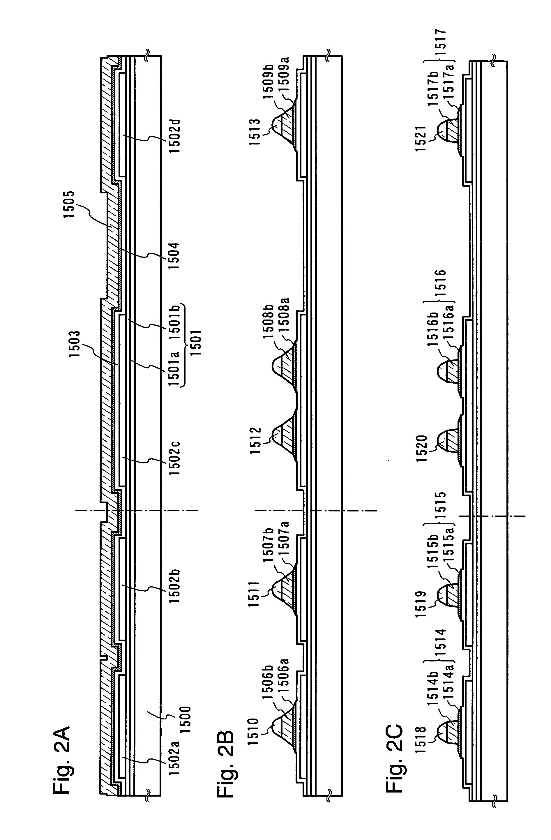
[0051] In the present embodiment, a method of manufacturing a light-emitting device according to the present invention is used to describe a method of manufacturing an active matrix display device that has a thin film transistor and a light-emitting element with reference to FIGS. 2A to 6B.

[0052] On a substrate 1500, a laminate of a base insulating film 1501a formed to have a film thickness from 50 to 100 nm and a base insulating film 1501b formed to have a film thickness from 50 to 100 nm is formed (FIG. 2A). The base insulating film 1501 (1501a and 1501b) is formed in order to prevent impurity diffusion from the substrate 1500 to a semiconductor layer. In the present embodiment, low alkali glass is used, and a silicon nitride film with a film thickness of 100 nm and a silicon oxide film with a film thickness of 100 nm are respectively formed by plasma CVD as the base insulating film 1501a and the base insulating film 1501b. Although the base insulating film ha...

embodiment 2

[0096] (Embodiment 2)

[0097] In the present embodiment, a display device that has a different structure from Embodiment 1 will be described with reference to FIG. 9.

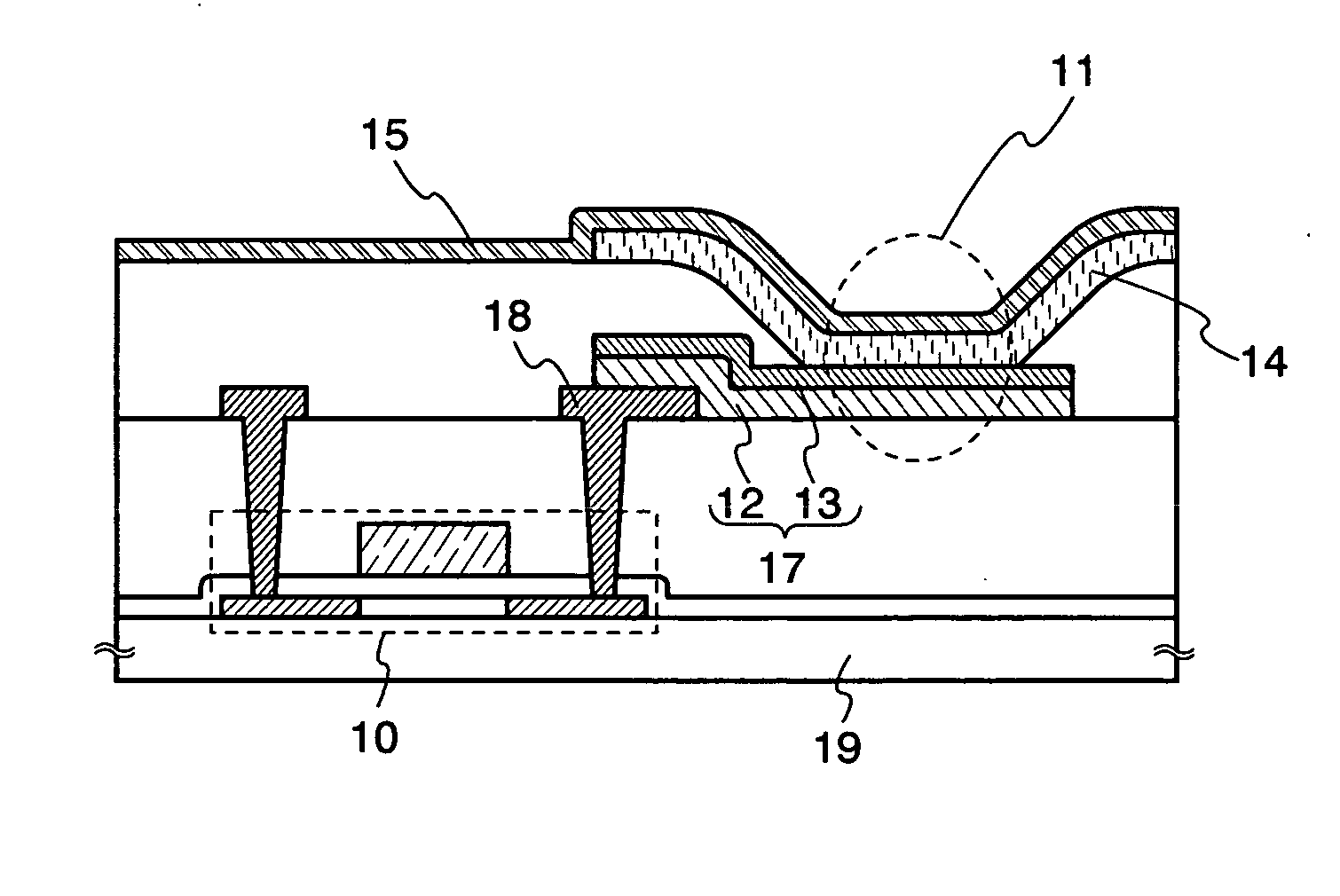
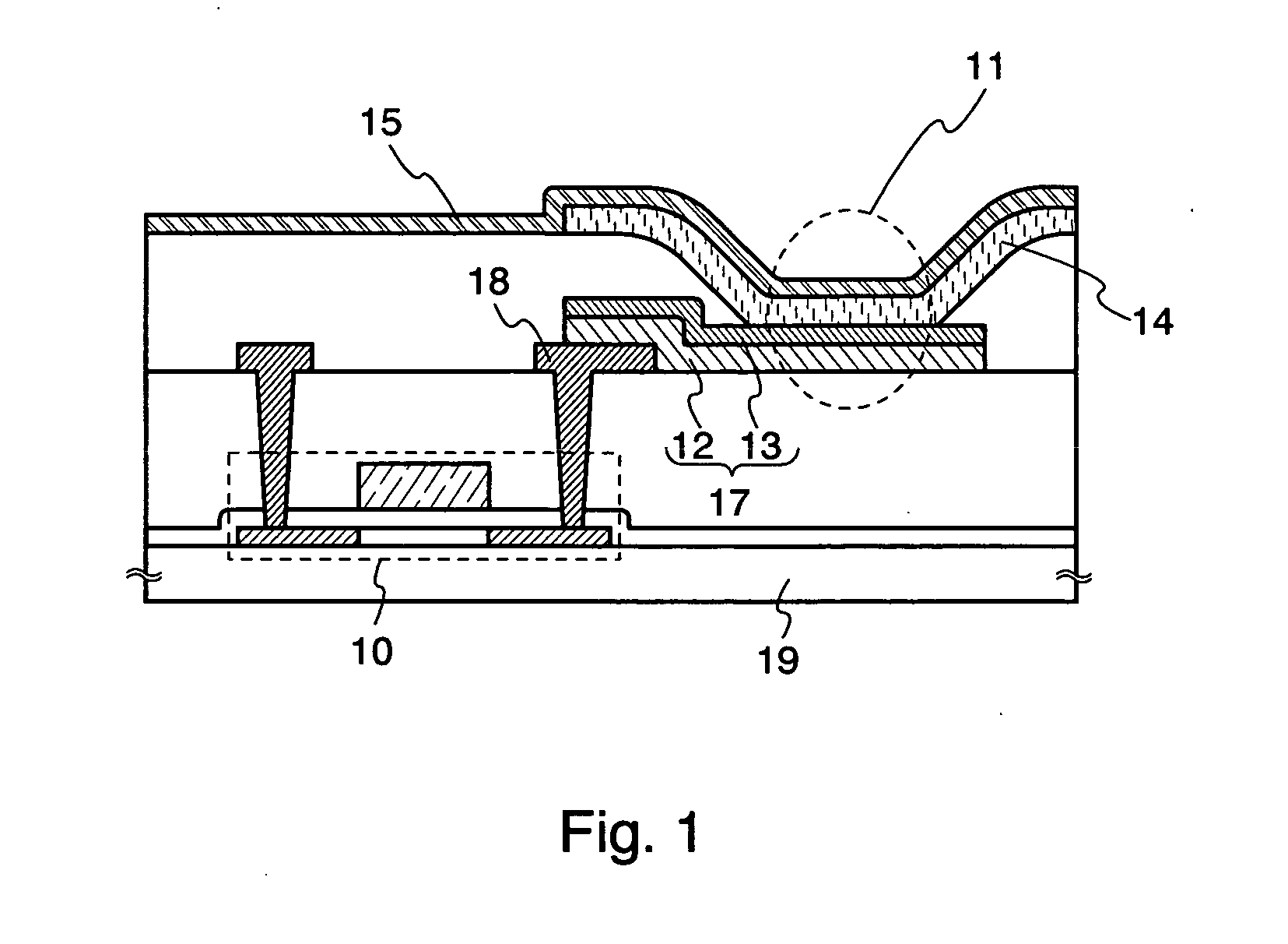
[0098] In FIG. 9, wirings (or electrodes) 1735 for transmitting electrical signals to respective TFTs are formed above an electrode 1738 of a light-emitting element, which is formed to have a first transparent conductive film 1736 and a second transparent conductive film 1737. In the case of the display device that has the foregoing structure, the wirings (or electrodes) 1735 are formed after forming the electrode 1738 of the light-emitting element. In FIG. 9, layers to be formed above the electrode 1738 of the light-emitting element such as an insulating film and a light-emitting layer are not shown.

[0099] Therefore, a solution such as a strong acid solution of iron chloride can be also used to process the first transparent conductive film 1736 and the second transparent conductive film 1737. However, in consideration of...

embodiment 3

[0102] (Embodiment 3)

[0103] In the present embodiment, a display device that has a different structure from Embodiments 1 and Embodiment 2 will be described with reference to FIG. 10.

[0104] In FIG. 10, wirings (or electrodes) 1835 for transmitting electrical signals to respective TFTs are provided on a first interlayer insulating film (1860 and 1861), a second interlayer insulating film (1862 and 1863) is provided on the wirings (or electrodes) 1835, and an electrode 1838 of a light-emitting element is provided on the second interlayer insulating film (1862 and 1863). The electrode 1838 of the light-emitting element includes a first transparent conductive film 1836 and a second transparent conductive film 1837. The second interlayer insulating film (1862 and 1863) has a two-layer structure of an organic resin film 1862 such as acrylic or polyimide and a silicon nitride film 1863 formed thereon by sputtering. In FIG. 10, layers to be formed above the electrode 1838 of the light-emitt...


PUM

PropertyMeasurementUnit
work functionaaaaaaaaaa
thicknessaaaaaaaaaa
specific resistanceaaaaaaaaaa

Abstract

It is an object of the present invention to provide a display device that has a structure of an electrode where a residue of a transparent conductive film is not generated when a weak acid solution is used in etching, which is particularly appropriate for an electrode of a light-emitting element. A display device according to the present invention has an electrode that has a laminated structure of laminated transparent conductive films, and the electrode has a first transparent conductive film as the bottom layer, where no residue is generated when a weak acid solution is used in etching, and a second transparent conductive film as the top layer, which has a work function of 5.0 eV or more.

Description

[0001] 1. Field of the Invention[0002] The present invention relates to a display device, in particular, to a structure of an electrode of an active matrix display device that has a light-emitting element.[0003] 2. Description of the Related Art[0004] In display devices such as an EL (Electro-Luminescence) display device and a liquid crystal display device, a transparent conductive film such as an indium tin oxide (ITO) film is used as an electrode of a pixel portion.[0005] As a method for processing an ITO film into a desired shape of an electrode, a method of performing wet etching with a resist film as a mask is mainly used.[0006] In general, concerning wet etching of an ITO film, it is known that an amorphous ITO film is subjected to wet etching more easily than a crystalline ITO film, and a structure of an electrode of a liquid crystal display device has been proposed in consideration of the etching characteristic (refer to Patent Document 1, for example).[0007] [Patent Documen...

Claims


Application Information

Patent Timeline
Patent Type & Authority Applications(United States)
IPC IPC(8): H01L21/77H01L21/84H01L27/12H01L27/32H01L51/52
CPCH01L27/3244H01L27/124H01L51/5206H10K59/12H10K50/816
Inventor AKIMOTO, KENGOMIYAGI, NORIKOEGUCHI, SHINGO
Owner SEMICON ENERGY LAB CO LTD
Why Eureka
Try Eureka