Solid state microchannel plate photodetector

Inactive Publication Date: 2004-12-09
YALE UNIV
View PDF4 Cites 115 Cited by
  • Summary
  • Abstract
  • Description
  • Claims
  • Application Information

AI Technical Summary

Benefits of technology

0068] FIG. 15 shows an alternative embodiment where the field effect is used to achieve Geiger mode

Problems solved by technology

It turns out that nearly all of the above limitations of SPADs occur, directly or indirectly, as a result of excessively high internal gain.
Since the o

Method used


Image

  • Solid state microchannel plate photodetector
  • Solid state microchannel plate photodetector
  • Solid state microchannel plate photodetector

Examples


Example

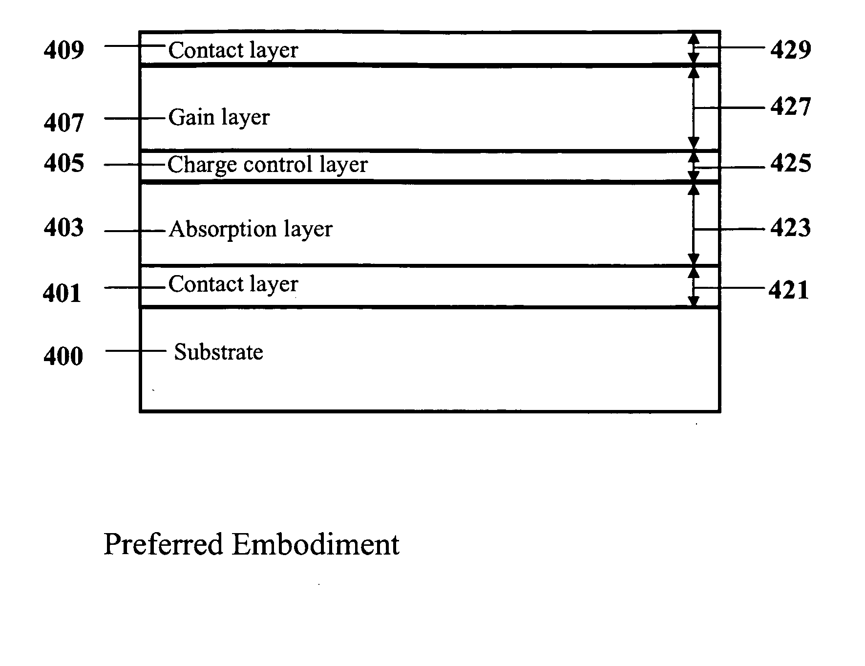
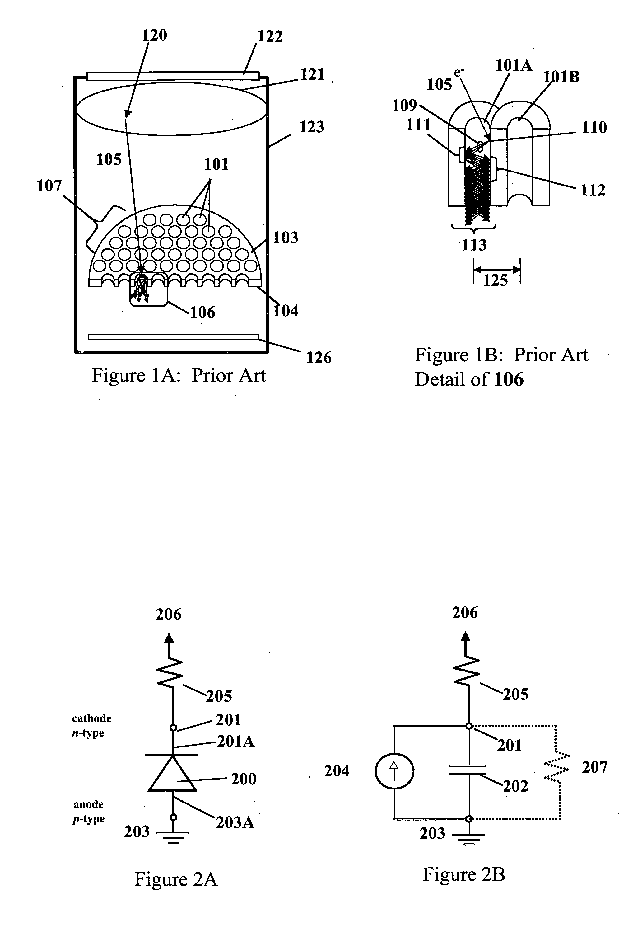
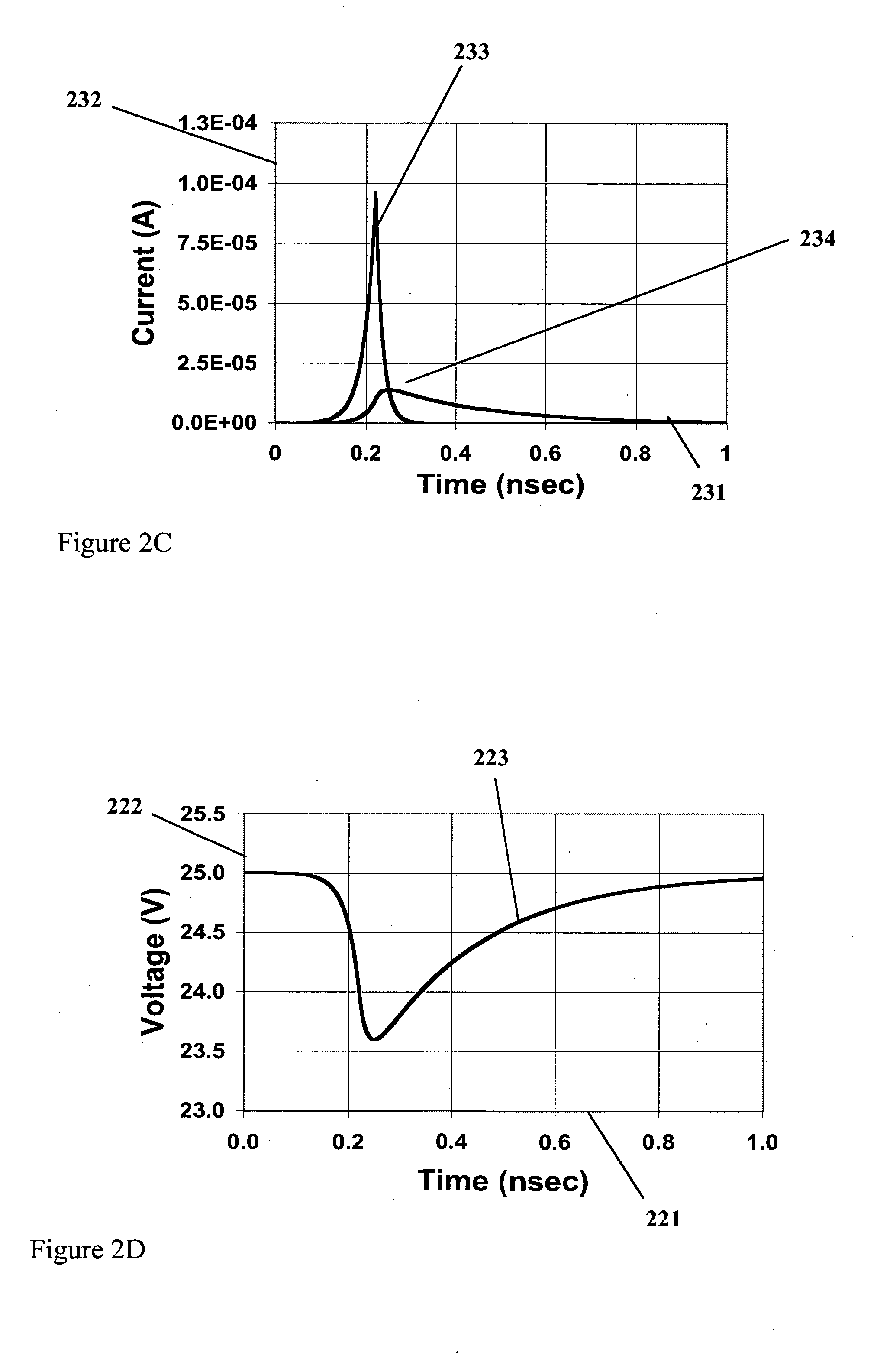
[0070] Reference is now made to FIG. 1A, showing a prior art approach to achieving high-speed, high sensitivity detection of optical photons using a microchannel plate electron multiplier. Since MCP operation requires a high vacuum, the interior of 123 must be evacuated. A window 122 allows incident photons 120 to enter into the vacuum environment of the MCP. When an incident photon 120 with sufficient photon energy strikes a photocathode 121, a photoelectron 105 is ejected into the vacuum. An electrical field is applied between the photocathode 121 and the top of the MCP electron multiplier 103 in order to accelerate photoelectron 105 towards the MCP 107. If photoelectron 105 gains sufficient energy from this electrical field, and if photoelectron 105 is incident on one of the pores 101 of the MCP 107, it may impact ionize at the sidewalls of the pores 101, resulting in a cascade of electrons in an efficient, low noise multiplication process. An electrical field is created within t...


PUM


Abstract

A solid state microchannel plate is disclosed comprising a multiplicity of photodetector elements, each using limited gain from a small Geiger mode avalanche and summing the contributions thereof. An array of such multiplicities operates as a pixelated linear or area photodetector. In the preferred embodiment, a multiplicity of passively quenched photodetector elements connect to a common anode, and each photodetector element is passively quenched by its own current-limiting resistor in series with its cathode.

Description

[0001] This application claims priority from the U.S. Provisional Patent Application "Solid State Photon Detector," filed May 1, 2003 as docket L3176-011, Ser. No. 60 / 467,090, incorporated herein by reference.[0002] This invention relates generally to the fields of solid state physics and electronics, more particularly to the design and fabrication of semiconductor photodetectors and photodetector arrays, and still more particularly to the design, fabrication and structure of elements of photodetectors, and arrays thereof, using avalanche gain.BACKGROUND OF THE INVENTION AND LIMITATIONS OF THE PRIOR ART[0003] The single-shot detection of low optical fluxes with frequency response at high frequency, at or near room temperature, generally requires gain in the photodetector itself, not just in a preamplifier following the photodetector. Internal gain is needed because the best prior art preamplifiers produce electrical noise equivalent to about 100 input-referred electrons per pulse fo...

Claims


Application Information

Patent Timeline
IPC IPC(8): G01J1/42G01J1/44H01L27/144H01L27/146H01L31/0232H01L31/0352H01L31/107
CPCG01J1/4228G01J1/44H01L27/1443H01L27/1446H01L27/14625H01L27/14627H01L27/14643H01L31/0232H01L31/03529H01L31/107H01L31/1075
Inventor HARMON, ERIC S.SALZMAN, DAVID B.
Owner YALE UNIV
Why Eureka
Try Eureka