Composite thin film holding substrate, transparent conductive film holding substrate, and panel light emitting body

a technology of transparent conductive film and holding substrate, which is applied in the direction of discharge tube/lamp details, natural mineral layered products, synthetic resin layered products, etc., can solve the problems of insufficient strength of thin film with a low refractive index, insufficient light discharge efficiency improvement effect by controlling light guiding, etc., to achieve strength and handling ease, the effect of improving the light discharge efficiency

Active Publication Date: 2004-12-16
SAMSUNG DISPLAY CO LTD
View PDF24 Cites 105 Cited by
  • Summary
  • Abstract
  • Description
  • Claims
  • Application Information

AI Technical Summary

Benefits of technology

0020] Accordingly, it is expected that the light-emitting efficiency can be improved by forming a thin film on the surface of a substrate independently of the kind of the subs...

Problems solved by technology

Thus, the effect of improving the light discharge efficiency by controlling light guiding is insufficient.
Further, there arises another problem in that, since lights are diffused by the light-diffusing layer (16), lights are mixed which makes it hard to obtain sharp contrast when it is needed that emitted lights should be recognized as an im...

Method used


Image

  • Composite thin film holding substrate, transparent conductive film holding substrate, and panel light emitting body
  • Composite thin film holding substrate, transparent conductive film holding substrate, and panel light emitting body
  • Composite thin film holding substrate, transparent conductive film holding substrate, and panel light emitting body

Examples


example 1

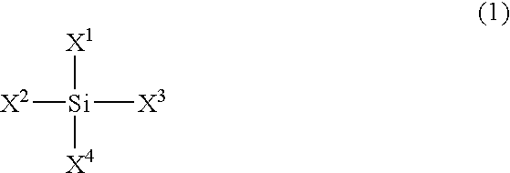
[0166] A solution was prepared by adding, to tetraethoxysilane (208 parts by mass), methanol (356 parts by mass), water (18 parts by mass) and 0.01N hydrochloric acid (18 parts by mass), and sufficiently mixing them with Disper. The resulting solution was stirred at 25.degree. C. in a constant temperature bath for 2 hours to obtain a SILICONE RESIN-M (a product obtained by hydrolyzing tetra-ethoxysilane and condensation-polymerizing the hydrolyzed product) as a binder-forming material having a weight-average molecular weight of 850. To the SILICONE RESIN-M was added hollow silica IPA-dispersed sol (solid content: 20 mass %, dispersion medium: isopropylalcohol, average primary particle diameter: about 35 nm, and shell thickness: about 8 nm, manufactured by CATALYSIS & CHEMICALS INDUSTIRES CO., LTD.) as the fine and hollow silica particles so that a mass ratio of the fine and hollow silica particles / SILICONE RESIN-M (converted to the condensed compound) based on the solid contents was...

example 2

[0168] To tetramethoxysilane (152 parts by mass) was added methanol (64 parts by mass), and the mixture was sufficiently stirred with Disper to obtain a solution of a binder-forming material for forming a silica aerogel binder. To this solution (216 parts by mass) were added methanol (64 parts by mass), water (36 parts by mass), 28 mass % of ammonia (0.6 parts by mass) and a 50-fold concentrated polystyrene fine particle-dispersed sol (solid content: 1 mass %, and average primary particle diameter: about 100 nm, manufactured by Duke Scientific), and the mixture was stirred to obtain a coating material composition which contained 10 mass % of the fine polystyrene particles in the mixture.

[0169] Next, the coating material composition was applied to a surface of a glass plate as a substrate with a spin coater at 1,000 rpm to form a coating film. After gelation of the coating film, it was dried under supercritical conditions of 80.degree. C. and 160 kg / cm.sup.2 to obtain a composite thi...

example 3

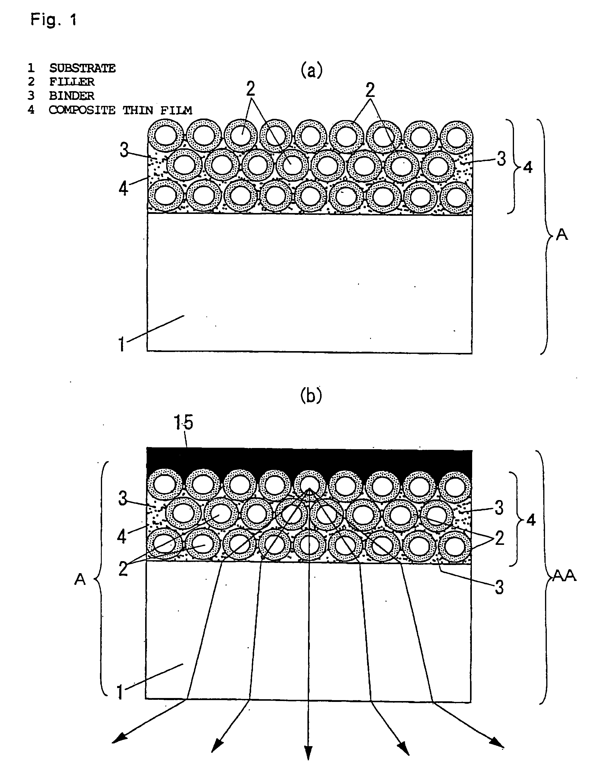
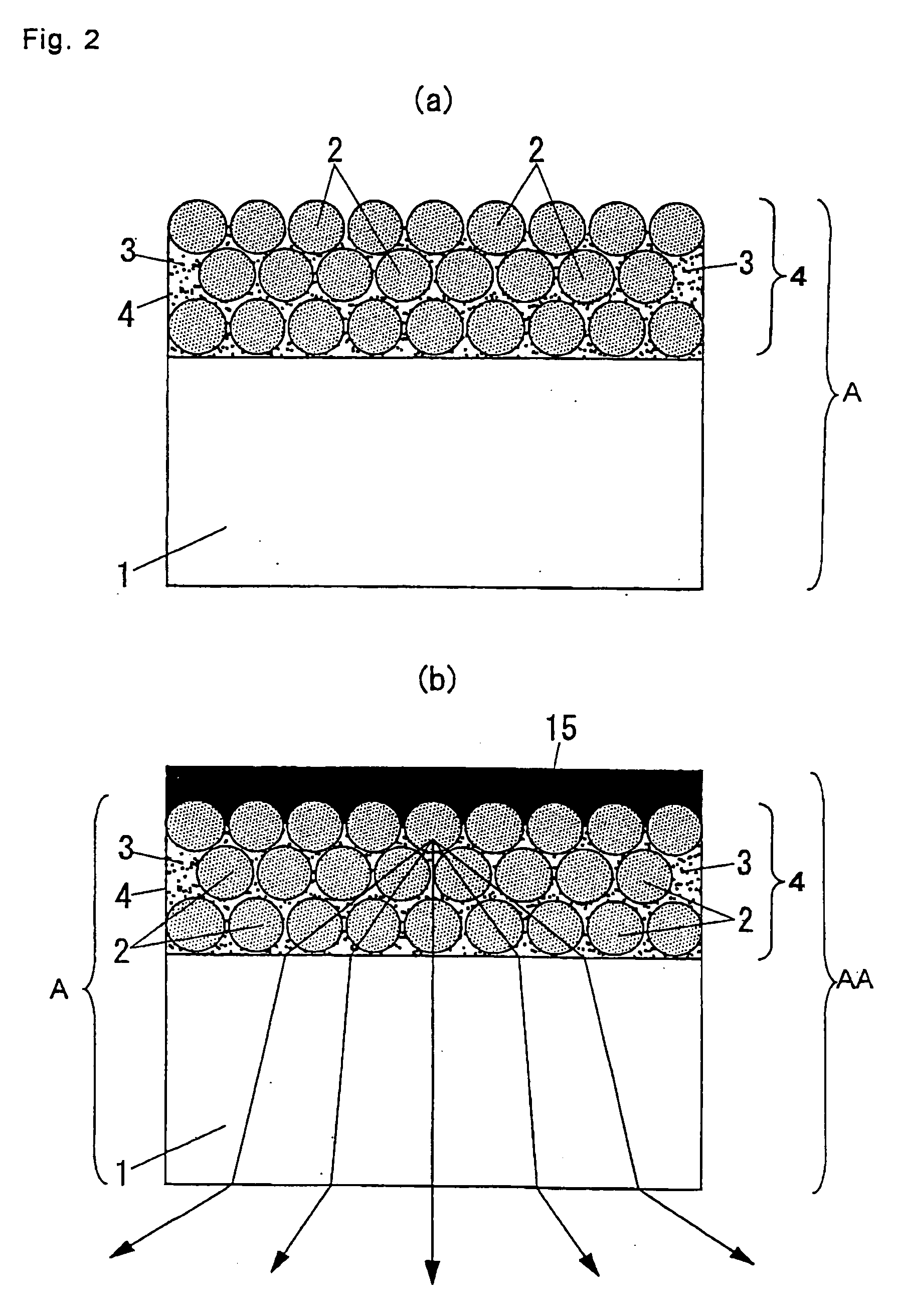
[0174] Plasma CVD was carried out at 300.degree. C. using tetraethoxysilane as a material source, so as to form a smoothening backing layer of a SiO.sub.2 film with a thickness of 100 nm on the surface of the composite thin film of the composite thin film-holding substrate obtained in Example 1. Next, RF sputtering was carried out at 200.degree. C., so as to form on the smoothening backing layer a transparent and electrically conductive film consisting of an ITO thin film with a thickness of 100 nm. Thus, a transparent and electrically conductive film-holding substrate as shown in FIG. 4(a) was obtained.


PUM

PropertyMeasurementUnit
Particle diameteraaaaaaaaaa
Fractionaaaaaaaaaa
Fractionaaaaaaaaaa

Abstract

There is provided a composite thin film-holding substrate in which a composite thin film (4) comprising a filler (2) having a refractive index lower than that of a substrate (1) and a binder (3) having a refractive index higher than that of the filler (2) is formed on a surface of the substrate (1). Light is efficiently scattered when passing through the composite thin film (3) which comprises the filler (2) and the binder (3) having different refractive indexes from each other. In addition, the refractive index of a composite thin film (4) comprising a filler (2) having a low refractive index is low. As a result, the discharge efficiency of light which passes through the composite thin film (4) from the substrate (1) to the external is improved.

Description

[0001] The present application is filed claiming the benefits provided in the Paris Convention, based on Japanese Patent Application No. 2001-327878 (filed on Dec. 25, 2001, titled "Coating Material Compositions and Articles Coated with the Same") and Japanese Patent Application No. 2001-327878 (filed on Dec. 25, 2001, titled "Composite Thin Film Substrate, Transparent Conductive Substrate and Surface Light Emitting Device"), and the contents described in the above applications are partially incorporated herein to form a part of the present description by reference in their entirety.[0002] The present invention relates to a surface light emitting device (or light emitting body) for the use in a variety of displays, display elements, backlights for liquid crystal displays or the like, and a composite thin film-holding substrate (or film-formed substrate) and a transparent electrically conductive film-holding substrate (or film-formed substrate) for the use in the surface light emitti...

Claims


Application Information

Patent Timeline
IPC IPC(8): B32B7/02B32B27/20C09D7/61C09D7/65G02B1/10G02B5/02H01J5/16H01L51/00H01L51/52
CPCC08K3/36Y10T428/265C08L2205/20C09D7/1291G02B1/10G02B5/0236G02B5/0242G02B5/0247G02B5/0278H01J5/16H01J2211/44H01L51/0096H01L51/5268Y02E10/549Y10T428/259Y10T428/24942Y10T428/25C08K7/22C09D7/70Y10T428/31663C09D7/65C09D7/61H10K77/10H10K50/854H05B33/22G02B1/11
Inventor YOKOGAWA, HIROSHIYOKOYAMA, MASARUKAWANO, KENJIITOU, NORIHIROTAKAHAMA, KOICHIYAMAKI, TAKEYUKITSUJIMOTO, AKIRAKISHIGAMA, YASUHISAIDE, NOBUHIRO
Owner SAMSUNG DISPLAY CO LTD
Why Eureka
Try Eureka