However, shrinking the dimensions of MOSFETs (
Metal Oxide Semiconductor Field Effect Transistors), i.e., main components of such semiconductor circuits induces various kinds of problems.
Due to high sensitivity of the
threshold voltage of the small size MOSFETs on the channel length, even a slight variation of channel length (i.e., the
gate length) leads to undesirable change of a
threshold voltage from the value intended at the time of the designing of the semiconductor circuit and eventually impairs the entire function of the circuit.
It entails that, since the value of the
threshold voltage strongly depends on the size of the gate
electrode, a slight
process variation may not be tolerated to obtain an intended electronic function and extremely tight control of the
process conditions is necessitated to achieve successful manufacturing.
This is very inconvenient for the manufacturing of a semiconductor circuit, such as a
DRAM (
Dynamic Random Access Memory), which requires a large number of highly uniform elements.
However, shallower pn junctions leads to an increase in the electric resistance of the source and drain electrodes, which hinders the high-speed transmission of electric signals.
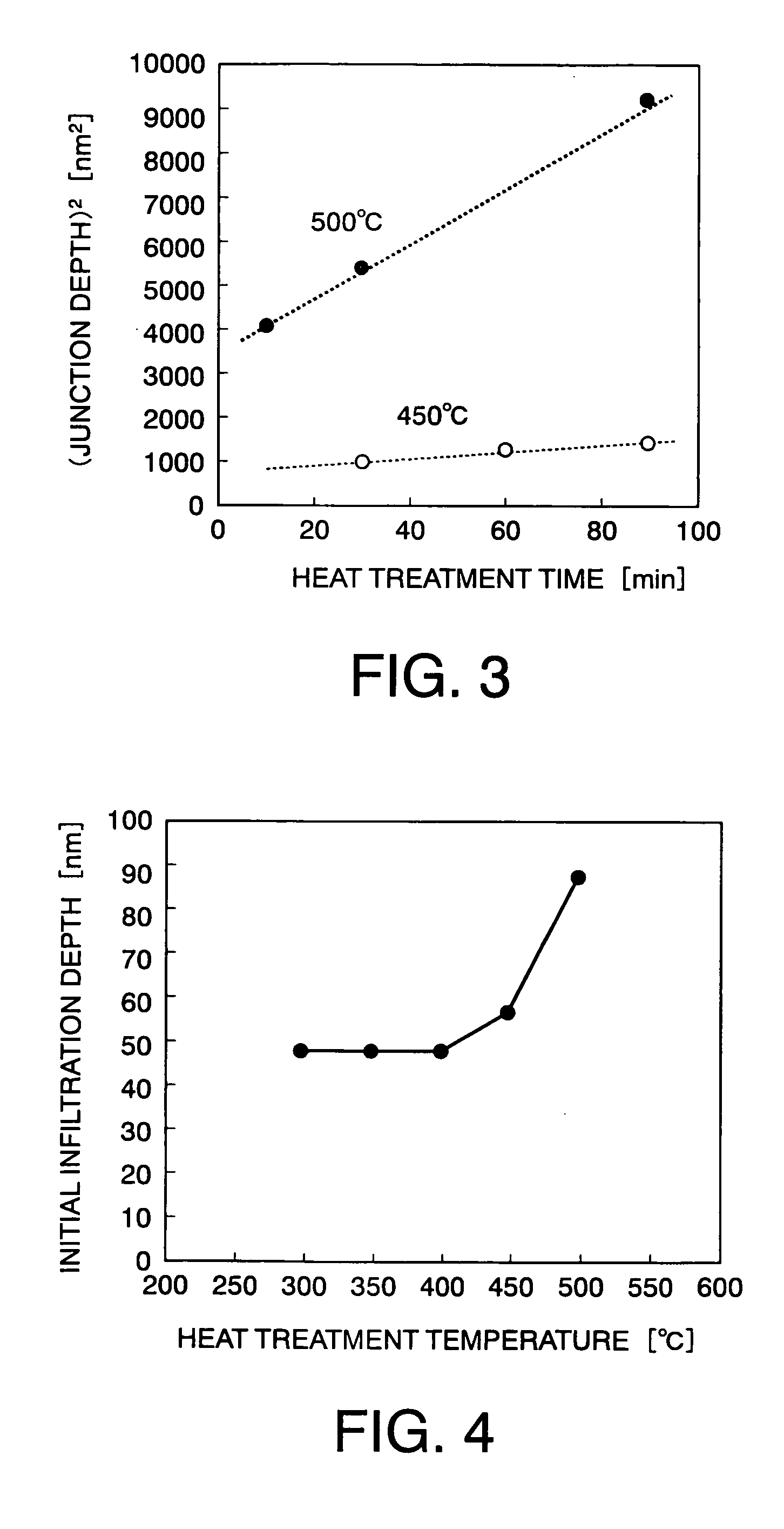
The technique claims that the formation of the
iridium intermediate layer increases the
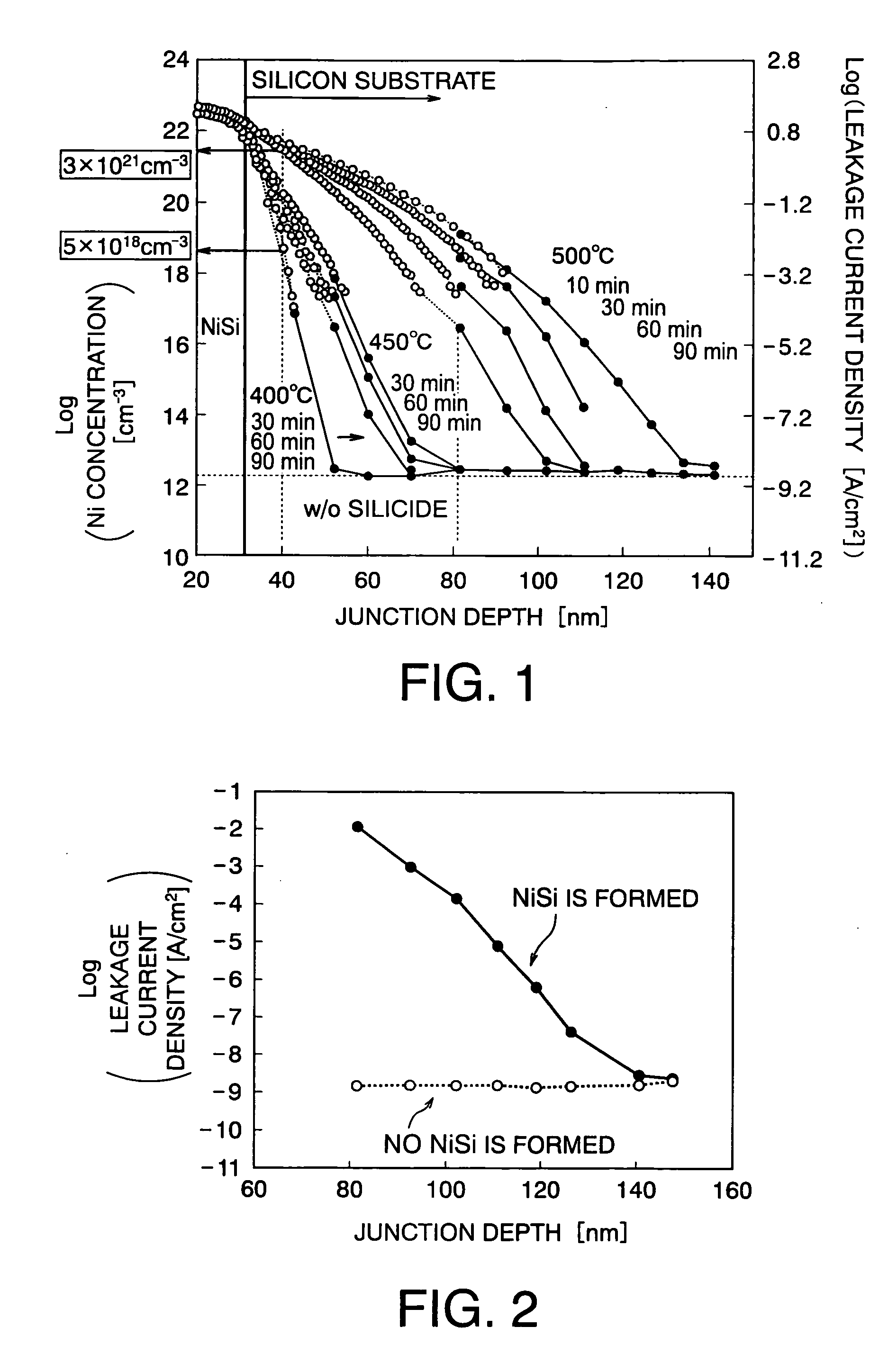
phase transition temperature from NiSi to NiSi.sub.2, resulting in leakage suppression even at a temperature of 850.degree. C.
However, without such a special treatment, a rapid
diffusion of
metal atoms is unavoidable at the interface between a
metal and
silicon, as described above.
When leakage currents flow through the source and drain junctions, the performance of the device is degraded.
In the case of a storage element such as a
DRAM, the information stored therein is erased, and the primary function of the
semiconductor device is lost.
If the junction depth does not reach the channel surface, the drivability of the
MOSFET is severely compromised.
On the other hand, when the junction depth is considerably deeper than the channel surface, a short-channel effect becomes a problem.
However, the epitaxial growth technique is very sensitive to the
surface conditions where the selective growth is to be performed.
When the thickness of the additional
silicon layer is not uniform, it is impossible to adjust the pn junction depth of all devices precisely to the original semiconductor
substrate surface (i.e., the surface where a channel is formed).
Non-uniform thickness means variable positions of the original semiconductor surface relative to the additionally formed
silicon surfaces, thus no way of accurate ajustment.
In addition, when the quality of the additionally formed silicon layer are not uniform, it becomes difficult to accurately position the pn junction at the intended location.
Since the speed of the
diffusion of impurities is modified (transient enhanced
diffusion) depending on the quality of the layer, if the quality of the silicon layer are not uniform, even when a predetermined thermal diffusion of impurities is applied in order to position the junction portions at the channel surface, the diffusion would proceed in an unexpected manner for each regions, resulting in non-uniform junction depths.
Even with the additional silicon layer, when the thickness or quality of the layer is not uniform, the metal atoms can easily penetrate the junction depth at a position of thin thickness or
poor quality, thereby causing a
junction leakage current.
However, for the aforementioned reasons, it is practically impossible to achieve a uniform and selective silicon growth of 150 nm-thickness.
Accordingly, with such a thickness, it becomes difficult to secure the electric isolation between the gate and the source and drain electrodes when silicidation reaction is made to proceed on these electrodes at a time (self-aligned silicidation, or
salicide process).
Thus, no matter how thick the selectively grown silicon layer is made at the other portions, its ability to block the leakage generation is not enhanced.
However, for silicidation of shallow junctions, the high-speed diffusion of metal atoms from the silicide induces substantial
junction leakage current.
However, formation of such a thick selective silicon layer of uniform thickness and
uniform quality has been very difficult.

