GaN substrate and method of fabricating the same, nitride semiconductor device and method of fabricating the same

Inactive Publication Date: 2004-12-30
SUMITOMO ELECTRIC IND LTD
View PDF8 Cites 169 Cited by
  • Summary
  • Abstract
  • Description
  • Claims
  • Application Information

AI Technical Summary

Problems solved by technology

However, the GaN substrate fabricated in this manner has the following problem: the GaN homoepitaxial layer is not normally grown on parts of the surface of the GaN substrate if the parts of the surface are contaminated.
Another cause thereof may be such dense-dislocation areas having a poor crystal quality.
Further, this publication does not disclose a GaN single crystal substrate including high dislocation regions and a low dislocation region that surrounds each high dislocation region.
The thickness of the intermediate layer 24 over the above range increases the possibility of occurrence of defects such as cracks.
The thickness of the intermediate layer

Method used


Image

  • GaN substrate and method of fabricating the same, nitride semiconductor device and method of fabricating the same
  • GaN substrate and method of fabricating the same, nitride semiconductor device and method of fabricating the same
  • GaN substrate and method of fabricating the same, nitride semiconductor device and method of fabricating the same

Examples


second example

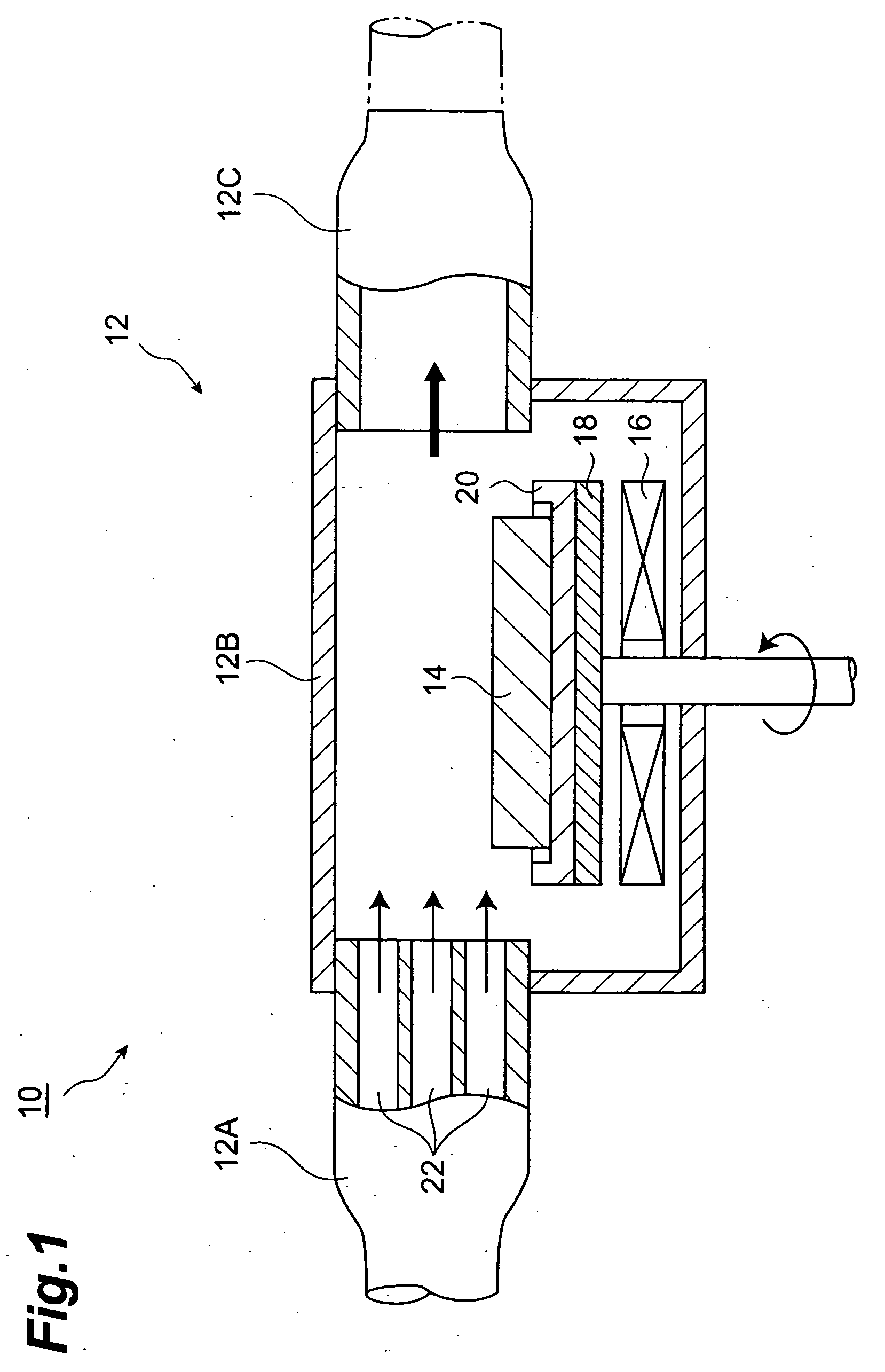
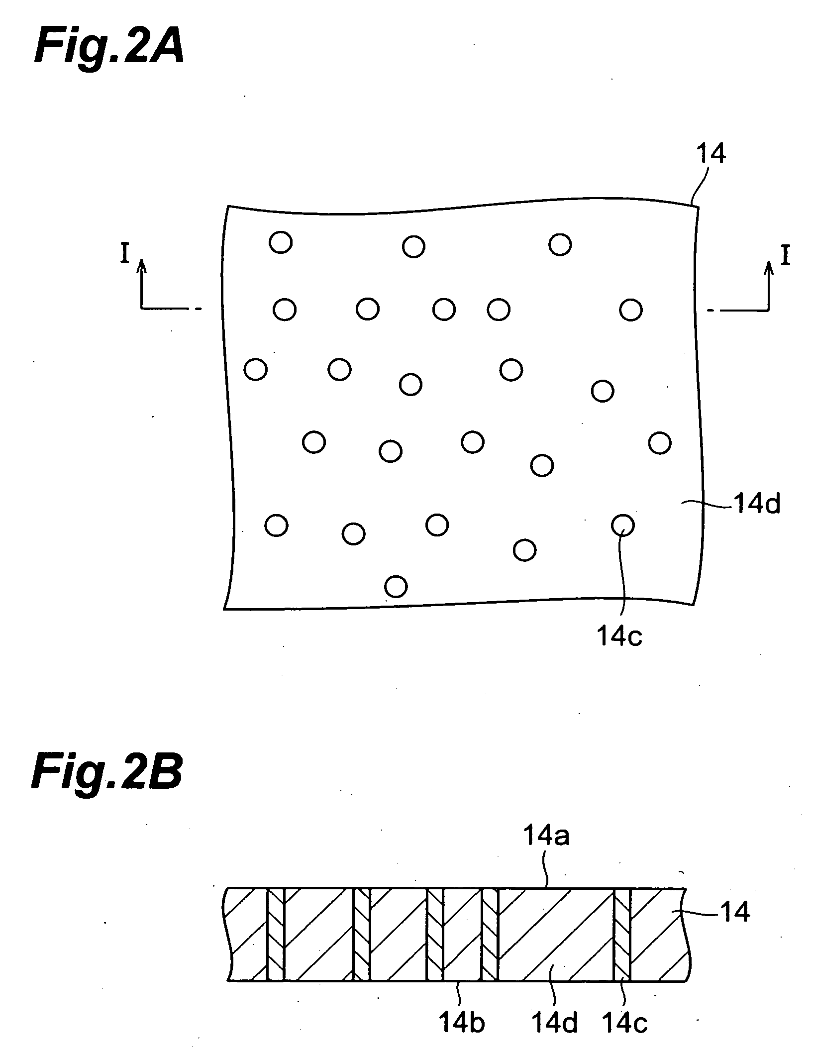
[0121] A blue light emitting device 1B has been fabricated as a second example. First, the substrate 14 is placed in the tray 20 and the surface 14a thereof is cleaned in the same manner as in the first example. Then, the substrate temperature and the furnace pressure is kept at Celsius 1050 degrees (.degree. C.) and at 101 kilopascals (kPa), respectively, and TMA, TMG, NH.sub.3 and SiH.sub.4 gases are supplied to the flow channel 12 to alternately deposit ten cycles of n-type Al.sub.0.14Ga.sub.0.86N layers in the thickness of 10 nanometers (nm) and n-type GaN layers in the thickness of 10 nanometers (nm), thereby growing an intermediate layer. Thereafter, an n-type buffer layer, a light emitting layer, a p-type cladding layer and a p-type contact layer are grown in the same manner as that in the first example. The surface of the p-type contact layer grown as above is observed with a differential interference microscope and this photograph reveals that the surface of the p-type cont...

experiment example

[0123] Subsequently, an experiment example for verifying the technical effects as shown in the above examples will be presented. A light emitting device without an intermediate layer has been formed as an example.

[0124] First, a GaN single crystal substrate is placed in the tray 20 on the susceptor 18 and the surface thereof is cleaned in the same manner as in the first example. Then, while keeping the substrate temperature at Celsius 1050 degrees (.degree. C.) and the furnace pressure at 101 kilopascals (kPa), TMG, NH.sub.3 and SiH.sub.4 are supplied the flow channel 12 to grow n-type GaN in the thickness of 2 micrometers (.mu.m). Thereafter, a light emitting layer, a p-type cladding layer, and a p-type contact layer are successively grown in the same manner as in the first example.

[0125] FIG. 12 is a view showing the surface of the p-type contact layer in the light emitting device fabricated as the experiment example. This is a photograph taken with a differential interference mic...
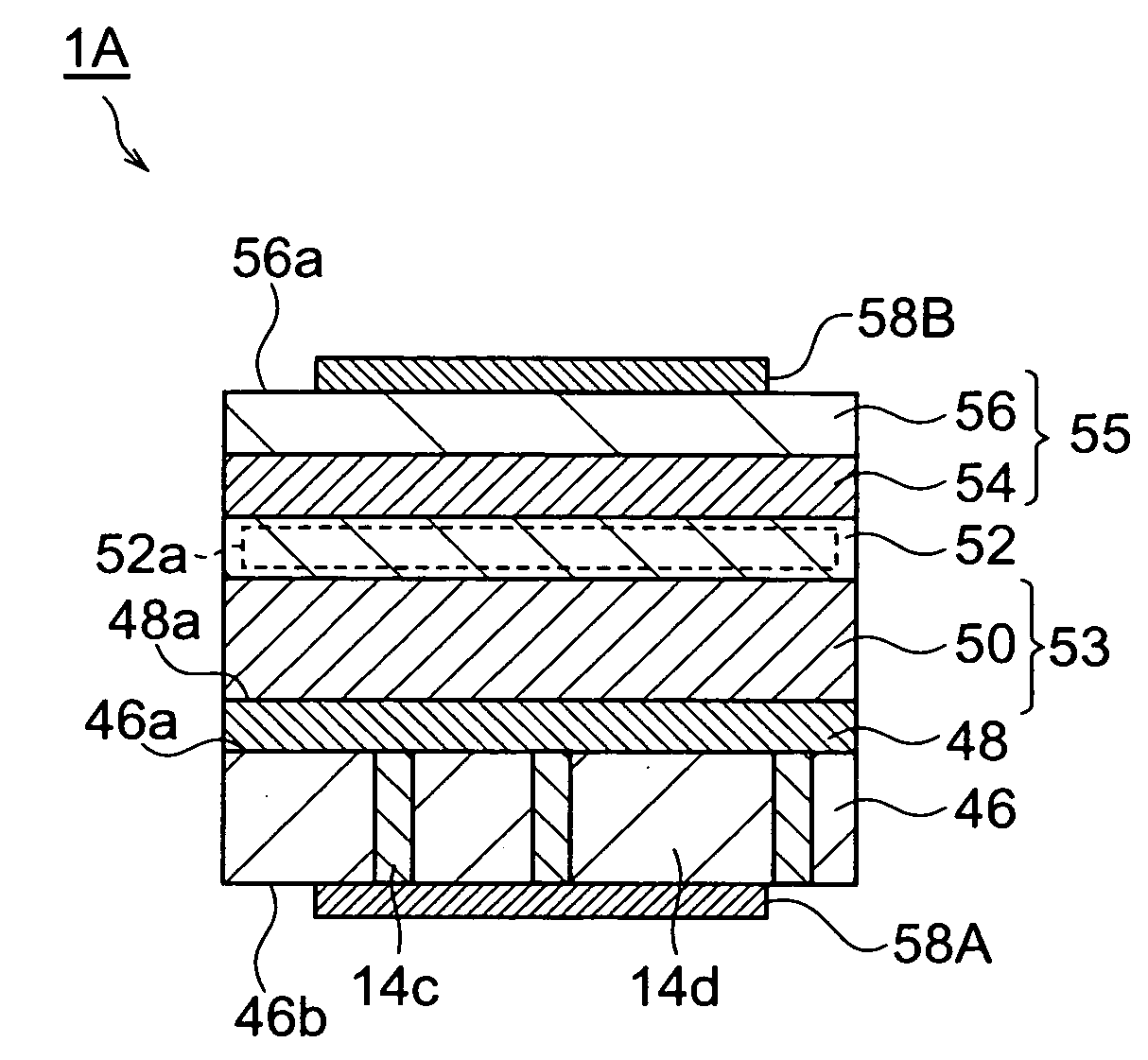
second embodiment

[0128] In the second embodiment, the n-type semiconductor region is formed on the intermediate layer and the p-type semiconductor region is formed on the active layer, but it is also possible that the p-type semiconductor region is formed on the intermediate layer and that the n-type semiconductor region is formed on the active layer.

[0129] The second embodiment exemplifies the light emitting devices as nitride semiconductor devices of the present invention, but the present invention is not limited thereto and can also be suitably applied to transistors and others made of GaN based material having the n-type region and p-type region.


PUM


Abstract

A GaN substrate comprises a GaN single crystal substrate, an AlxGa1-xN intermediate layer (0<x<=1) epitaxially grown on the substrate, and an GaN epitaxial layer grown on the intermediate layer. The intermediate layer is made of AlGaN and this AlGaN grows over the entire surface of the substrate with contaminants thereon and high dislocation regions therein. Thus, the intermediate layer is normally grown on the substrate, and a growth surface of the intermediate layer can be made flat. Since the growth surface is flat, a growth surface of the GaN epitaxial layer epitaxially grown on the intermediate layer is also flat.

Description

[0001] 1. Field of the Invention[0002] The present invention relates to a GaN epitaxial substrate and a method of fabricating the same and to a nitride semiconductor device and a method of fabrication the same.[0003] 2. Related Background Art[0004] Gallium nitride (GaN) is attractive material of substrates for light emitting devices. For example, Japanese Patent Application Laid-Open No. 2001-102307 publication discloses the formation of a GaN substrate. In this formation of GaN substrates, a GaN thick layer is grown by the lateral growth method on a semiconductor single-crystal substrate such as a gallium arsenide (GaAs) substrate. Then, the GaAs substrate is removed from the GaN thick layer and one or more GaN substrates are formed from the GaN thick layer.[0005] Prior to manufacturing semiconductor devices thereon, an epitaxial layer is grown on such a GaN substrate to form a GaN epitaxial substrate. As disclosed in Japanese Patent Application Laid-Open No. 2000-340509 publicatio...

Claims


Application Information

Patent Timeline
IPC IPC(8): C30B25/02H01L33/06C30B25/18H01L21/20H01L21/205H01L29/20H01L33/32
CPCC30B25/02C30B25/183C30B29/403C30B29/406H01L21/02389H01L21/02458H01L21/0254H01L21/0262H01L29/2003H01L33/007H01L21/20
Inventor AKITA, KATSUSHITAKASUKA, EIRYONAKAYAMA, MASAHIROUENO, MASAKIMIURA, KOUHEIKYONO, TAKASHI
Owner SUMITOMO ELECTRIC IND LTD
Why Eureka
Try Eureka