Photovoltaic cell assembly and the method of producing one such assembly

a photovoltaic cell and assembly technology, applied in the direction of pv power plants, solid-state devices, accounting/billing services, etc., can solve the problems of non-negligible cell breakage risks, large consumption of silver- and aluminium-based solder paste, and high cost of manufacturing, so as to reduce manufacturing costs and reduce cell efficiency

Inactive Publication Date: 2005-01-06
APOLLON SOLAR SAS
View PDF9 Cites 93 Cited by
  • Summary
  • Abstract
  • Description
  • Claims
  • Application Information

AI Technical Summary

Benefits of technology

[0013] The object of the invention is to remedy these shortcomings and more particularly to provide an assembly of photovoltaic cells enabling the problems of degradation of the cell efficiency to be overcome. The assembly must preferably also have a very low manufacturing cost.

Problems solved by technology

This type of fabrication process implies a large consumption of very expensive silver- and aluminium-based solder paste.
The soldering itself is a costly, mechanically complicated operation requiring the cell to be turned and able to result in non-negligible risks of breakage of the cell.
In case of misalignment, the cell is liable to be destroyed when soldering takes place and the shadow factor on the front face may be increased.
It is moreover difficult to perform soldering operations on the same positions on the front and rear faces and the contacts already soldered on one of the faces are liable to become unsoldered when soldering is performed on the other face.
All known assemblies present a mediocre resistance to water vapour diffusion to the silicon, which decreases the conversion efficiency of the cells within a few years.
A no more than mediocre thermal conduction of the polymer can also be noted which leads to an increase of the temperature and a reduction of the efficiency.
Soldering of the strips and assembly of the cells also constitutes a handicap as they are long operations able to break the cells and result in a high production cost.

Method used


Image

  • Photovoltaic cell assembly and the method of producing one such assembly
  • Photovoltaic cell assembly and the method of producing one such assembly
  • Photovoltaic cell assembly and the method of producing one such assembly

Examples


Embodiment Construction

.

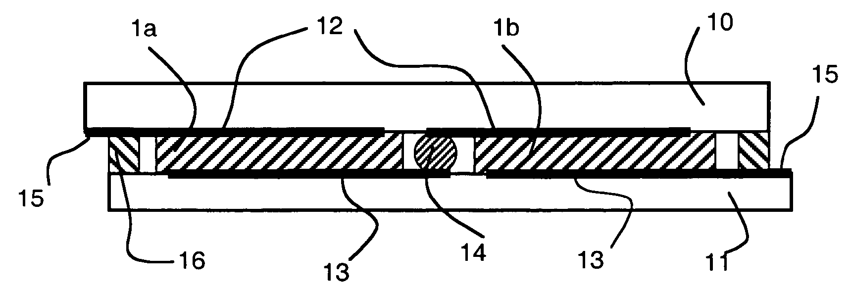
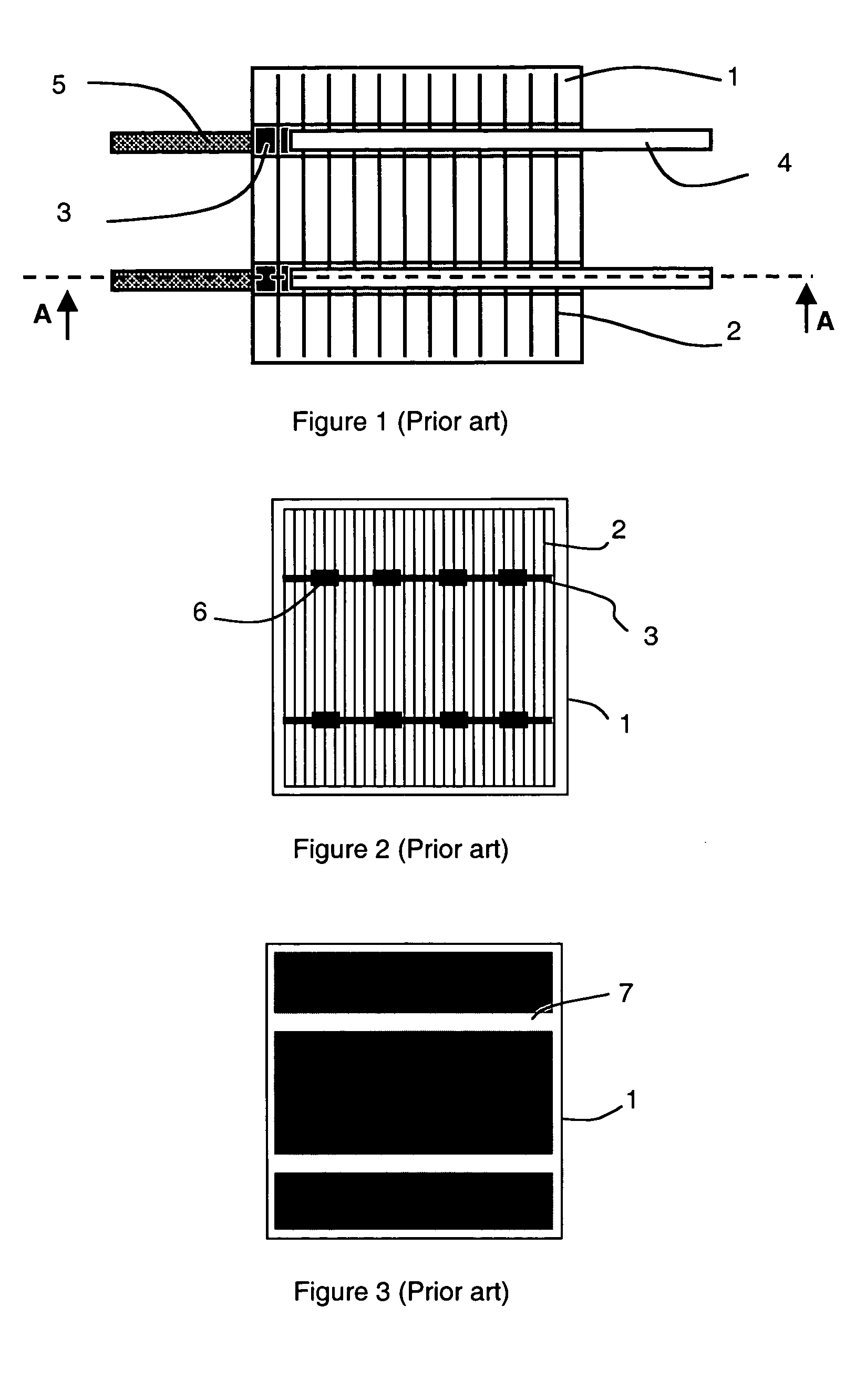
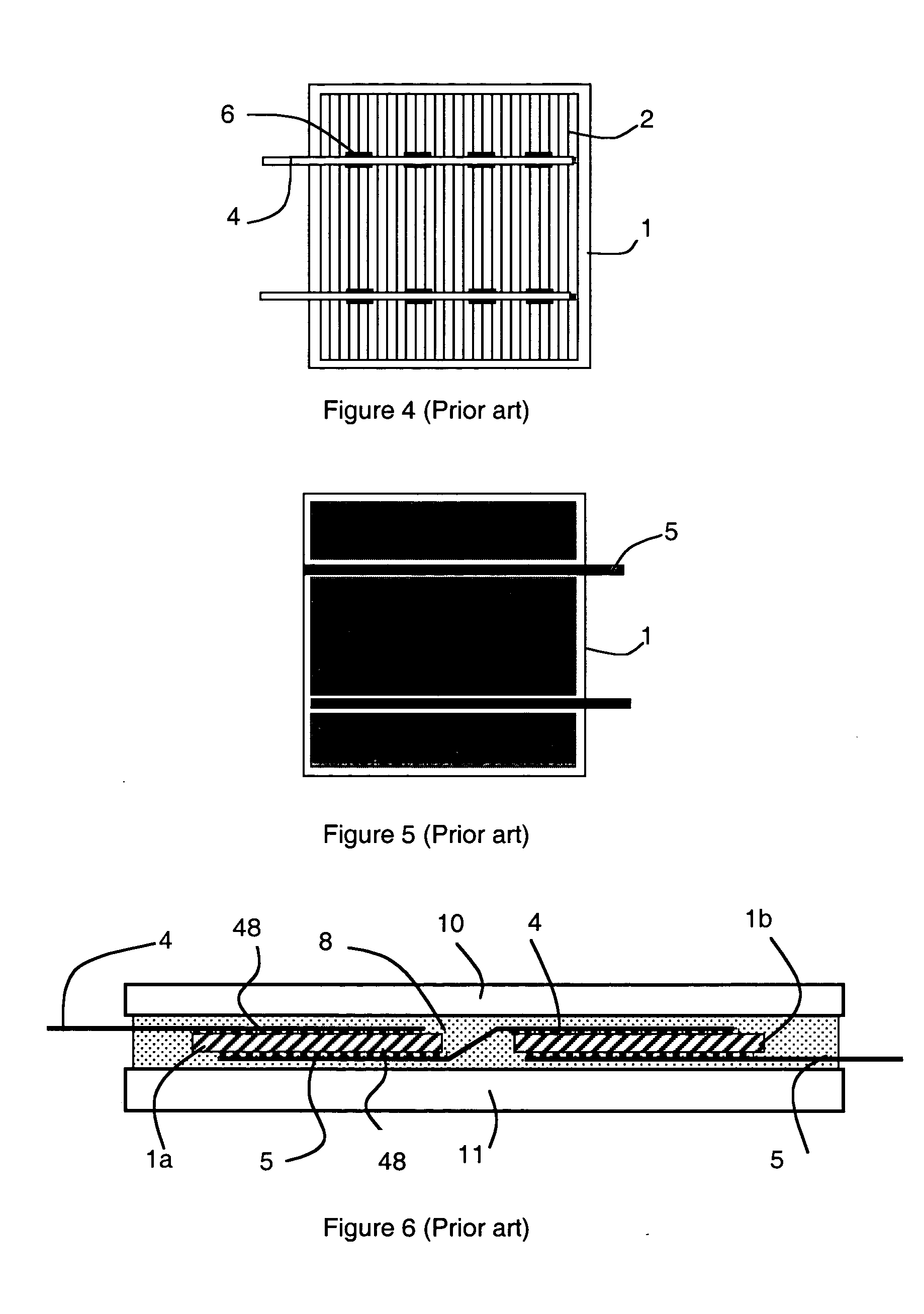
[0042]FIGS. 7 and 8 respectively illustrate the front face and rear face of a cell 1 according to the invention before encapsulation. The front face only comprises the network of fine electrodes 2, from 50 to 120 μm in width. The collector buses 3 and solder studs 6 can be eliminated, which enables the surface taken up by metallization to be reduced, and thus enables the light absorption and consequently the current and power generated by the cell to be increased while reducing the consumption of metal used, in particular silver paste. The rear face comprises a second network of electrodes, generally denser or, as represented in FIG. 8, a metal layer, preferably made of aluminium, practically covering the whole of the rear surface, which enables the performances of the cell to be increased by creation of a rear field. As the solder tracks 7 are eliminated, the cost of a cell is thus decreased both by reduction of the quantity of silver necessary and by simplification of the fabrica...


PUM


Abstract

The photovoltaic cells (1a, 1b) of the assembly are disposed side by side between a front (10) and rear (11) glass substrates and are connected in series by means of front (12) and (13) rear connecting conductors and of interconnection elements (14). The connecting conductors can be formed on the internal face of each glass substrate facing the location of each of the cells or obtained by laser cutting, through the glass substrates, of conducting strips tightened beforehand between the cells and the glass substrates. The electrical interconnection elements (14) are disposed between two adjacent cells (1) to connect the opposite connecting conductors associated to two adjacent cells. A sealing joint (16), made of inorganic material, arranged between the two glass substrates (10, 11), defines a sealed internal volume which contains all the cells (1). Sealing is performed between 380° C. and 480° C. for a period of less than 30 minutes.

Description

BACKGROUND OF THE INVENTION [0001] The invention relates to an assembly of photovoltaic cells arranged side by side between front and rear glass substrates and connected in series by front and rear connecting conductors respectively arranged on each side of each of the cells and comprising a connecting zone extending beyond a predetermined side of said location, the assembly comprising electrical interconnection elements arranged between two adjacent cells to connect the opposite connecting zones of the front and rear connecting conductors respectively associated to two adjacent cells. STATE OF THE ART [0002] A photovoltaic cell is conventionally formed on a bulk silicon substrate cut into the form of wafers with a thickness of a few hundred microns. The substrate can be made of mono-crystalline silicon, polycrystalline silicon, or semi-conducting layers deposited on a glass or ceramic substrate. It has on its surface a network of narrow electrodes, generally made of silver or alumi...

Claims


Application Information

Patent Timeline
Patent Type & Authority Applications(United States)
IPC IPC(8): H01L31/048H01L31/05H04M17/00
CPCH01L31/048H04M17/00H04M17/20H04M2215/2026H04M2215/32H01L31/0508Y02E10/50H01L31/02008H01L31/02013H01L31/022433H04W4/24H01L31/0488
Inventor BARET, GUYLAUVRAY, HUBERT
Owner APOLLON SOLAR SAS
Why Eureka
Try Eureka