Method, chemistry, and apparatus for noble metal electroplating on a microelectronic workpiece

a noble metal and workpiece technology, applied in the direction of electrical equipment, electrolysis process, electrolysis components, etc., can solve the problems of substantial film stress near the contact location, non-uniform deposition of plated metallic materials, and detrimental to the function and reliability of microelectronic components produced using these materials. , to achieve the effect of low film stress

Inactive Publication Date: 2005-01-06
SEMITOOL INC
View PDF43 Cites 21 Cited by
  • Summary
  • Abstract
  • Description
  • Claims
  • Application Information

AI Technical Summary

Benefits of technology

[0022] The present invention is directed to an improved electroplating method, chemistry, and production worthy apparatus for depositing noble metals onto the surface of the workpiece, such as a semiconductor wafer, pursuant to manufacturing a microelectronic device, circuit, and / or component. The reliability of the noble metal material deposited using the disclosed method, chemistry, and / or apparatus is significantly better than the reliability of noble metal structures deposited using the teachings of the prior art. This is largely attributable to the low stress of films that are deposited using the teachings disclosed herein. The metals, which can be deposited, include gold, silver, platinum, palladium, ruthenium, iridium, rhodium, osmium and alloys containing these metals.
[0025] In accordance with a still further aspect of the present invention, an apparatus for plating a noble metal on a microelectronic workpiece is disclosed that comprises a reactor chamber that contains an electroplating solution having ions or complexes of the noble metal or noble metal alloy that is to be plated onto the workpiece. The apparatus also includes a workpiece support including a contact assembly for providing electroplating power to a surface at a side of the workpiece that is to be plated and an anode spaced from the workpiece support within the reaction chamber and contacting the electroplating solution. A chemical delivery system is employed for supplying the electroplating solution to the reactor chamber and recirculating electroplating solution removed from the reactor chamber. To eliminate fouling of the solution, as is quite prevalent when plating a noble metal, a multi-stage filtration system is utilized. The filtration system is disposed within the chemical delivery system for filtering electroplating solution removed from the reactor chamber before it is re-supplied to the reactor chamber. It includes at least a first filter stage for filtering particles greater than or equal to a first size and a second filter stage disposed downstream of the first filter stage for filtering particles greater than or equal to a second size, the first size being greater in magnitude than the second size.
[0026] It may be desirable to use a current thief in any of the foregoing electroplating apparatus. In accordance with a still further aspect of the present invention, a disposable current thief is set forth. The disposable current thief is disposed in the electroplating solution between the anode and the contact assembly and is formed from the conductive portions of a printed circuit board. The disclosed current thief is manufactured from readily available materials using simple manufacturing processes thereby significantly reducing the costs of providing current thieving in noble metal electroplating processes.

Problems solved by technology

This stress can be detrimental to the function and reliability of the microelectronic components produced using these materials.
This non-uniform distribution of current across the wafer, in turn, causes non-uniform deposition of the plated metallic material and, further, produces a substantial film stress near the contact locations.
Such reactors are therefore not particularly well-suited for plating noble metals, such as platinum.
Another problem with electroplating of noble metals onto workpieces concerns efforts to prevent the electric contacts themselves from being plated during the electroplating process.
However, noble metals such as platinum, unlike metals such as copper, cannot be reverse plated from the electrical contacts.
As a result, current thieving, while desirable to increase film uniformities, can be costly to implement.
Electroplated material may not adhere well to the exposed barrier layer material, and is therefore prone to peeling off in subsequent wafer processing steps.
Further, metal that is electroplated onto the barrier layer within the reactor may flake off during the electroplating process thereby adding particulate contaminants to the electroplating bath.
Such contaminants can adversely affect the overall electroplating process.
The specific metal used for the seed layer can also complicate the electroplating process.
As a consequence, use of the typical plurality of electrical wafer contacts (for example, six (6) discrete contacts) may not provide adequate uniformity of the plated metal layer on the wafer due to non-uniformities in the plating current that result from the high electrical resistance of the seed layer and / or noble metal layer (e.g., platinum).
Beyond the contact related problems discussed above, there are also other problems associated with electroplating reactors.
Still further, existing electroplating reactors are often difficult to maintain.

Method used


Image

  • Method, chemistry, and apparatus for noble metal electroplating on a microelectronic workpiece
  • Method, chemistry, and apparatus for noble metal electroplating on a microelectronic workpiece
  • Method, chemistry, and apparatus for noble metal electroplating on a microelectronic workpiece

Examples


Embodiment Construction

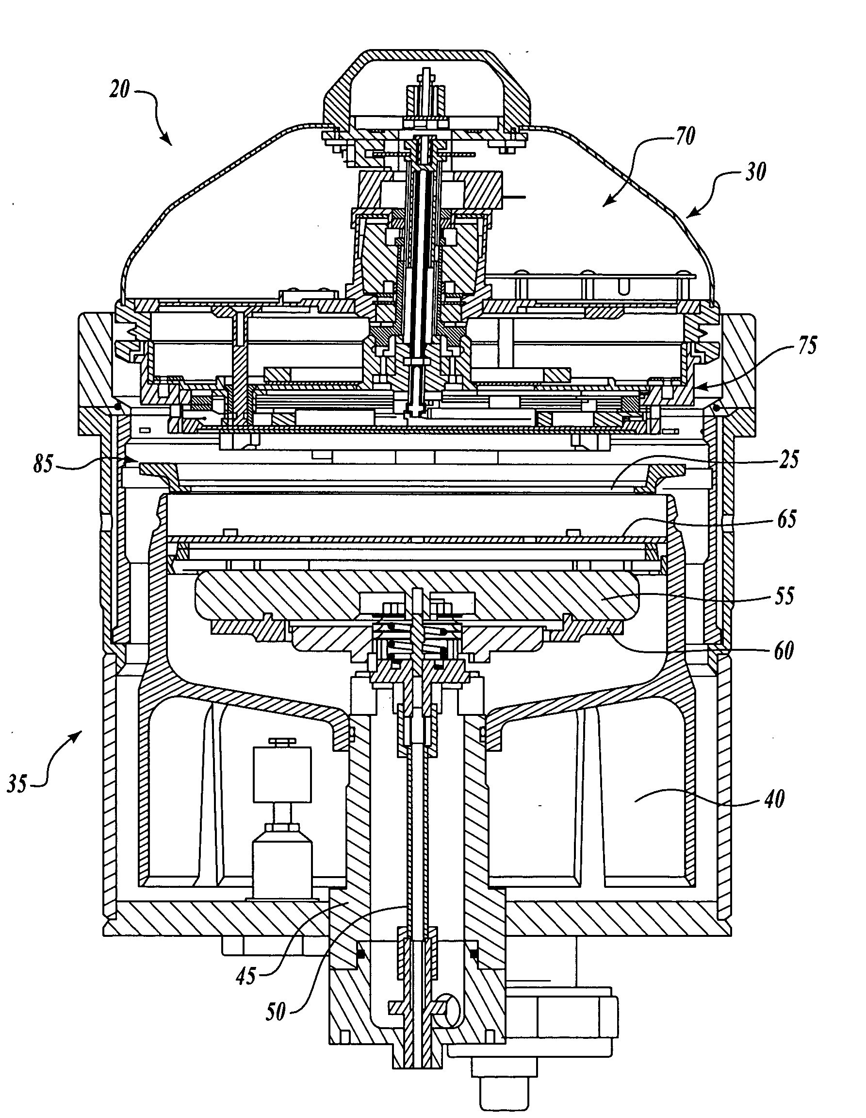
[0044] With reference to FIGS. 1-3, there is shown a reactor assembly 20 for electroplating a noble metal on the surface of a microelectronic workpiece, such as a semiconductor wafer 25. Generally stated, the reactor assembly 20 is comprised of a reactor head 30 and a corresponding reactor bowl 35. This type of reactor assembly is particularly suited for effecting electroplating of semiconductor wafers or like workpieces, in which an electrically conductive, thin-film seed layer of the wafer is electroplated with a blanket or patterned noble metal layer, such as a layer of platinum.

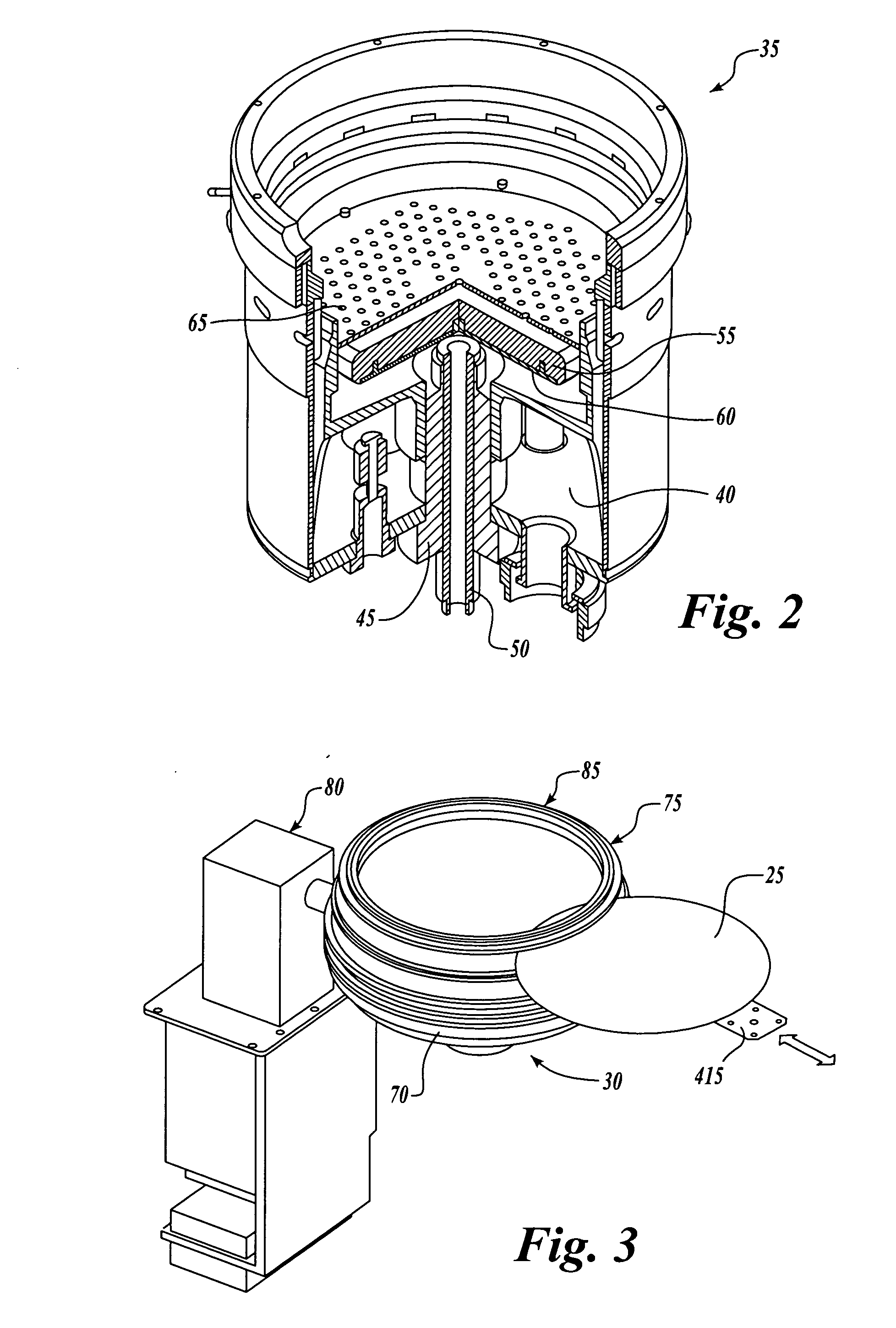
[0045] A specific construction of one embodiment of a reactor bowl 35 suitable for use in the reactor assembly 20 is illustrated in FIG. 2. The electroplating reactor bowl 35 is that portion of the reactor assembly 20 that contains electroplating solution, and that directs the solution at a high flow rate against a generally downwardly facing surface of an associated workpiece 25 to be plated. To this en...


PUM

PropertyMeasurementUnit
current densityaaaaaaaaaa

Abstract

The present invention is directed to an improved electroplating method, chemistry, and production worthy apparatus for depositing noble metals (e.g., platinum) and their alloys onto the surface of the workpiece, such as a semiconductor wafer, pursuant to manufacturing a microelectronic device, circuit, and / or component. The reliability of the noble metal material deposited using the disclosed method, chemistry, and / or apparatus is significantly better than the reliability of noble metal structures deposited using the teachings of the prior art. This is largely attributable to the low stress of films that are deposited using the teachings disclosed herein. The metals, which can be deposited, include gold, silver, platinum, palladium, ruthenium, iridium, rhodium, osmium and alloys containing these metals.

Description

CROSS-REFERENCE TO RELATED APPLICATION [0001] This application is a divisional of copending Application Ser. No. 09 / 429,446. filed Oct. 28, 1999.FIELD OF THE INVENTION [0002] The present invention relates to a method of reducing stress in electroplated noble metals. BACKGROUND OF THE INVENTION [0003] The present invention is directed to electroplating a low-stress noble metal film onto the surface of a workpiece, such as a semiconductor wafer, in the manufacture of microelectronic devices and / or components. More particularly, the present invention is directed to a method, chemistry and apparatus for electroplating a noble metal, such as platinum, on a microelectronic workpiece. [0004] Production of semiconductor integrated circuits and other microelectronic devices from workpieces, such as semiconductor wafers, typically requires formation of one or more metal layers on the workpiece. These metal layers are used, for example, to electrically interconnect the various devices of the i...

Claims


Application Information

Patent Timeline
Patent Type & Authority Applications(United States)
IPC IPC(8): C25D7/12H01L21/288
CPCC25D17/001C25D7/123
Inventor GRAHAM, LYNDON W.JACOBSON, CURT W.RITZDORF, THOMAS L.
Owner SEMITOOL INC
Why Eureka
Try Eureka