Carrier detecting circuit and infrared communication device using same

a carrier detection and infrared communication technology, applied in the direction of transmission, gain control, transmission monitoring, etc., can solve the problems of circuits increasing, impedance of transistors, general difficulty of integrators 123/b>, etc., and achieve the effect of reducing the capacitance of integration capacitors

Inactive Publication Date: 2005-01-06
SHARP KK
View PDF6 Cites 16 Cited by
  • Summary
  • Abstract
  • Description
  • Claims
  • Application Information

AI Technical Summary

Benefits of technology

The present invention has an objective to provide a carrier detecting circuit capable of reducing a capacitance of an integration capacitor without causing problems that a

Problems solved by technology

It has been generally difficult for the integrator 123 to obtain high response characteristics with respect to a minute current.
However, if the operating currents i101 and i102 are low currents of not more than 10 nA, the

Method used


Image

  • Carrier detecting circuit and infrared communication device using same
  • Carrier detecting circuit and infrared communication device using same
  • Carrier detecting circuit and infrared communication device using same

Examples


Embodiment Construction

The following will explain an embodiment of the present invention with reference to FIGS. 1 through 3, and 9 through 11.

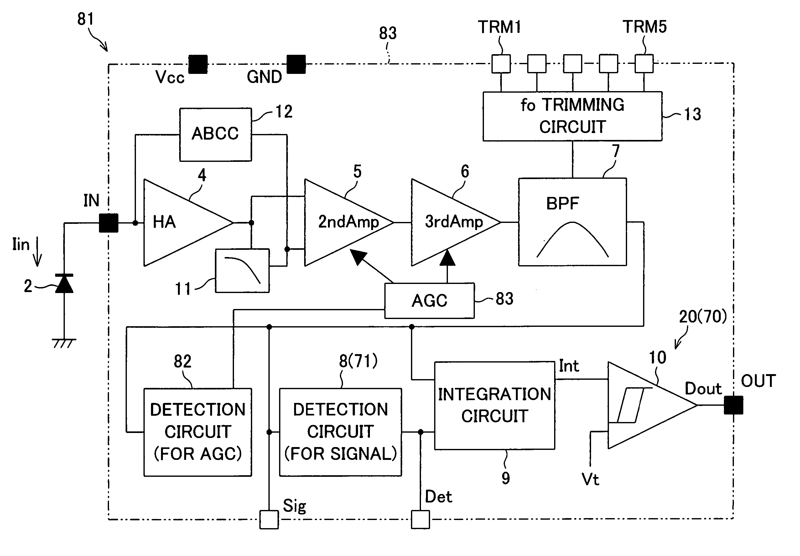
First, an arrangement of a receiver that includes a carrier detecting circuit in accordance with the present embodiment will be briefly explained. FIG. 9 is a block diagram showing an arrangement example of an infrared remote controller receiver 1 which is an infrared communication device. FIG. 10 is waveform charts of sections in the receiver 1. The receiver 1 is so arranged that an external photodiode 2 converts an infrared transmission code signal into a photocurrent signal Iin as shown in FIG. 10, and inputs the converted photo-current signal Iin to a receiving chip 3. Further, the receiving chip 3, which is an integrated circuit, demodulates the converted photocurrent signal Iin thus received and outputs a digital signal Dout to a microcomputer or other device which controls an electronic device. The infrared signal is an ASK (Amplitude Shift Keying) signal...


PUM


Abstract

A conventional carrier detecting circuit which generates a carrier detection level by integral action based on a reception signal and detects using the carrier detection level whether a carrier exists is arranged to charge and discharge in the following manner, an integration capacitor in an integrator that performs the integral action. Namely, the integration capacitor is (i) either charged or discharged in accordance with a result of the discrimination of the reception signal at the carrier detection level, or (ii) charged in accordance with the result of the discrimination while the integration capacitor is constantly discharged at a constant level. In contrast, a carrier detecting circuit of the present invention is arranged so that the integration capacitor is both charged and discharged constantly at a level that varies in accordance with the result of the discrimination. In other words, the integration capacitor is charged and discharged using a difference current between a current charged from a charging circuit and a current discharged to a discharging circuit. With this, it is possible to reduce the chip area without causing problems due to the reduction of the currents flowing through the transistors.

Description

FIELD OF THE INVENTION The present invention relates to a carrier detecting circuit suitably employed as a demodulator of a signal containing a carrier, and an infrared communication device that mounts the carrier detecting circuit for use in reception. BACKGROUND OF THE INVENTION Infrared communication devices capable of receiving infrared rays have been widely used, such as infrared remote controller receivers. In an infrared communication device, a received infrared transmission code signal is converted into an electric signal by a photodiode, for example, and then amplified. Then, in the infrared communication device, a bandpass filter extracts a predetermined carrier frequently component from the amplified signal, and a carrier detecting circuit determines in accordance with an output signal of the bandpass filter, whether or not a carrier exists, and then outputs a result of the determination. FIG. 12 is an equivalent circuit diagram showing an arrangement example of a carri...

Claims


Application Information

Patent Timeline
IPC IPC(8): H03G3/30H04L27/06H03D1/10
CPCH03G3/3084
Inventor INOUE, TAKAHIROTAKEUCHI, NOBORU
Owner SHARP KK
Why Eureka
Try Eureka