
System and method based on field-effect transistors for addressing nanometer-scale devices

Inactive Publication Date: 2005-01-13
CALIFORNIA INST OF TECH
View PDF15 Cites 12 Cited by
  • Summary
  • Abstract
  • Description
  • Claims
  • Application Information

AI Technical Summary

Benefits of technology

[0012] Many benefits are achieved by way of the present invention over conventional techniques. For example, some embodiments of the present invention provide a system and method for matching the nanometer-dimension patterning techniques and lithographic patterning techniques and for addressing each of the individual nanostructures. For example, the lithographic patterning techniques may use an optical beam such as in the ultraviolet range or the far-ultraviolet range or use an electron beam. Certain embodiments of the present invention can select and address a signal wire whose cross-section area is smaller than the resolution of lithographic techniques. Some embodiments of the present invention can select and address a signal wire from a plurality of signal wires, whose pitch is smaller than the resolution of lithographic techniques.
[0013] Certain embodiments of the present invention improves the density of an addressing system. The addressing structures patterned with lithographic techniques usually has a density lower than that of the nanostructures. For example, the addressing structures include address lines with gate regions and inactive regions. To improve overall density, it is desirable to reduce the number of addressing structures for a given number of nanostructures. For example, 2n nanostructures can be individually addressed by approximately n or 2×n addressing lines. n is a positive integer. Some embodiments of the present invention improve tolerance of manufacturing defects. The addressing system does not require manufacturing precision at the level of nanowires. For example, the addressing lines are much larger and spaced farther apart than the nanometer-scale wires. In another example, the spacing between the gate regions of the addressing lines is much larger than the spacing between the nanowires. In yet another example, the smallest gate region covers more than one nanowire.
[0014] Some embodiments of the present invention significantly increase the ease of fabrication. A predetermined registration is not required between a given gain region and a give nanowire. For example, the pattern of gain regions for an addressing line continues beyond the edges of the array of nanowires. Certain embodiments of the present invention reduce power consumption. Field effect transistors formed between the gate regions and the nanowires usually do not allow substantial electrical current between the addressing lines and the nanowires except limited leakage current. The reduction in power consumption also reduces heat generation. Additionally, the field effect transistors can serve as gain elements. Some embodiments of the present invention provides an addressing system and method for a large number of nanometer-scale devices without consuming an unacceptable level of power. Certain embodiments of the present invention can bring a nanowire to high resistivity state and low resistivity state depending upon applied gate voltage. Certain embodiments of the present invention improve etching selectivity between SiO2 and Si. The etching rate of SiO2 is much higher than that of Si. Some embodiments of the present invention can select and address an array of semiconductor wires on an insulating substrate.

Problems solved by technology

The binary tree multiplexer 100 may consume significant power and involve complicated fabrication processes.

Method used


Image

  • System and method based on field-effect transistors for addressing nanometer-scale devices
  • System and method based on field-effect transistors for addressing nanometer-scale devices
  • System and method based on field-effect transistors for addressing nanometer-scale devices

Examples


Embodiment Construction

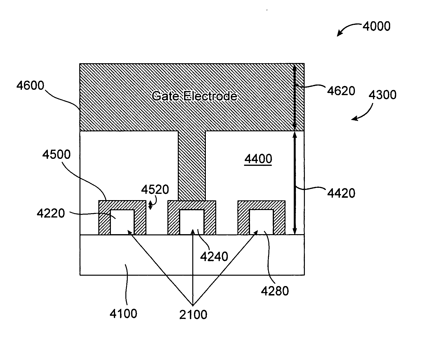
[0034] The present invention relates generally to the field of nanotechnology. More specifically, the invention provides a method and system based on field effect transistors for addressing nanometer-scale devices. Merely by way of example, the invention has been applied to nanometer-scale wires, but it would be recognized that the invention has a much broader range of applicability.

System for Addressing Devices

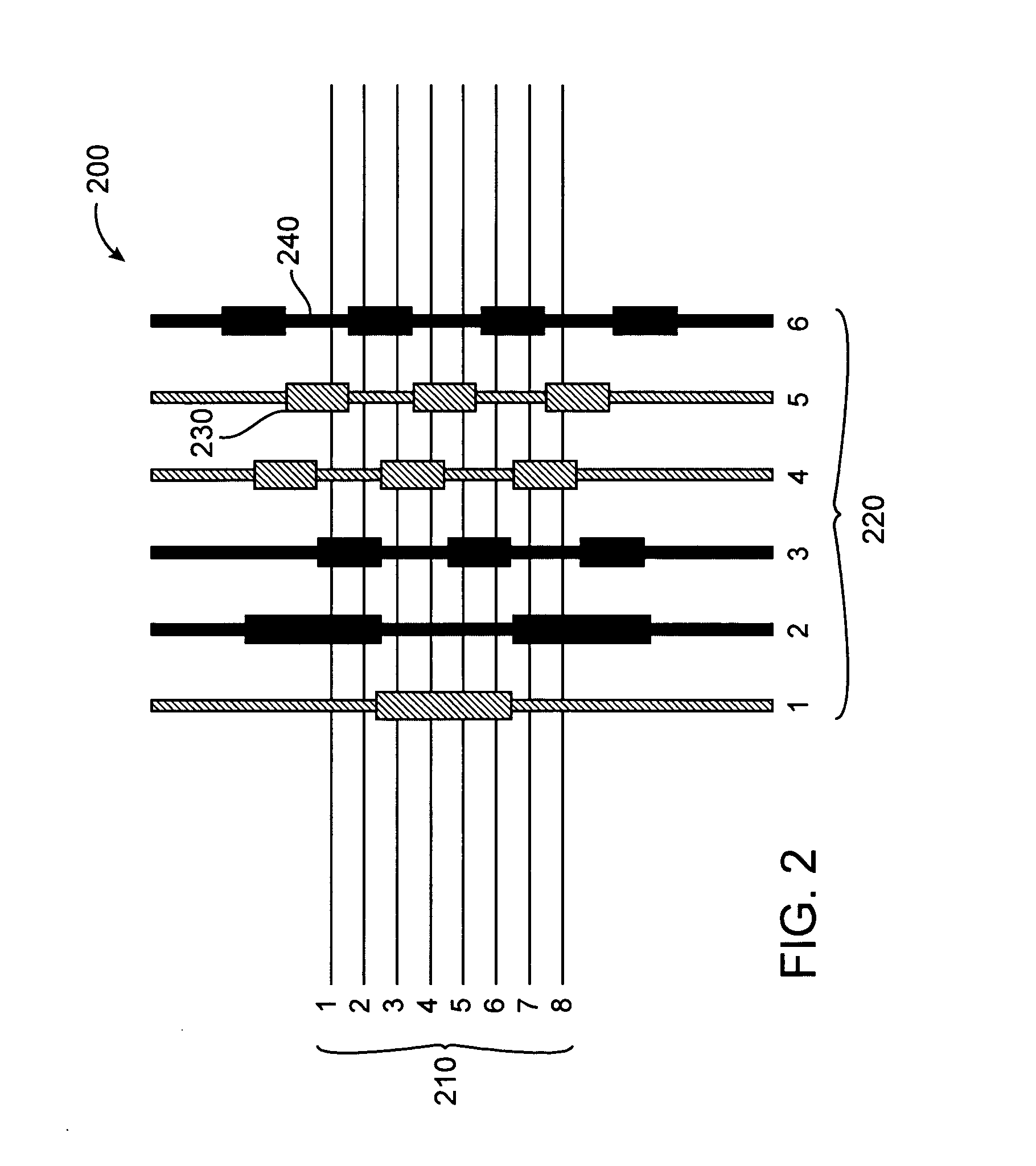
[0035]FIG. 2 is a simplified system for addressing nanometer-scale devices according to an embodiment of the present invention. The diagram is merely an example, which should not unduly limit the scope of the present invention. One of ordinary skill in the art would recognize many variations, alternatives, and modifications. The system 200 includes nanometer-devices 210 and address lines 220. Although the above has been shown using components 210 and 220, there can be many alternatives, modifications, and variations. Some of the systems may be combined. Other systems may be...


PUM


Abstract

A system and method for selecting nanometer-scaled devices. The method includes a plurality of semiconductor wires. Two adjacent semiconductor wires of the plurality of semiconductor wires are associated with a separation smaller than or equal to 100 nm. Additionally, the system includes a plurality of address lines. Each of the plurality of address lines includes a gate region and an inactive region and intersects the plurality of semiconductor wires at a plurality of intersections. The plurality of intersections includes a first intersection and second intersection. The first intersection is associated with the gate region, and the second intersection is associated with the inactive region.

Description

CROSS-REFERENCES TO RELATED APPLICATIONS [0001] This application claims priority to U.S. Provisional No. 60 / 480,888 filed Jun. 24, 2003, which is incorporated by reference herein.STATEMENT AS TO RIGHTS TO INVENTIONS MADE UNDER FEDERALLY SPONSORED RESEARCH OR DEVELOPMENT [0002] Work described herein has been supported, in part, by DARPA Grant No. ______. The United States Government may therefore have certain rights in the invention.REFERENCE TO A “SEQUENCE LISTING,” A TABLE, OR A COMPUTER PROGRAM LISTING APPENDIX SUBMITTED ON A COMPACT DISK. [0003] NOT APPLICABLE BACKGROUND OF THE INVENTION [0004] The present invention relates generally to the field of nanotechnology. More specifically, the invention provides a method and system based on field effect transistors for addressing nanometer-scale devices. Merely by way of example, the invention has been applied to nanometer-scale wires, but it would be recognized that the invention has a much broader range of applicability. [0005] In th...

Claims


Application Information

Patent Timeline
IPC IPC(8): H01LH01L21/31H01L21/469H01L21/84H01L27/10H01L27/12H01L27/14H01L29/06H01L29/49H01L29/82
CPCB82Y10/00G11C2213/81H01L21/84H01L27/10H01L27/1203H01L29/0665H01L2924/0002H01L29/0673H01L29/4908H01L29/785H01L2924/00
Inventor HEATH, JAMES R.LUO, YIBECKMAN, ROB
Owner CALIFORNIA INST OF TECH
Learn More