Semiconductor packages for enhanced number of terminals, speed and power performance

a technology of which is applied in the direction of semiconductor devices, semiconductor/solid-state device details, electrical apparatus, etc., can solve the problems of limiting the number of connections that can be made on the available chip surface, limiting the achievable bump pitch, and increasing the difficulty of preserving clean signals without mutual interference. , to achieve the effect of high pin count, high speed and power performance, and high speed

Inactive Publication Date: 2005-01-13
TEXAS INSTR INC
View PDF10 Cites 32 Cited by
  • Summary
  • Abstract
  • Description
  • Claims
  • Application Information

AI Technical Summary

Benefits of technology

[0011] Embodiments of the present invention are related to high pin count devices intended for high speed and power performance. It is a technical advantage that the invention offers the device designer several independent parameters to achieve high speed, control signal integrity and inductance, and increase power performance. The parameters include the number and separation of the signal, power and ground planes, the widths of the connector lines, the location of the package I / O terminals relative to the chip contact pads, and the choice and electrical characteristics of the interconnection elements. One or more embodiments of the invention offer choices including small gold bumps, more massive reflow bumps, and controlled wire bonding. Furthermore, several of these choices make the device less sensitive to environmental influences or temperature variations.

Problems solved by technology

Higher levels of integration include the need for higher numbers of signal lines and power lines, yet smaller feature sizes make it more and more difficult to preserve clean signals without mutual interference.
Second, flip-chip assembly often provides higher interconnection densities between chip and package than wire bonding.
In known technology, however, the achievable bump pitch is limited.
These limits severely restrict the number of connections that can be made on the available chip surface, and constrain the use of flip-chip techniques for devices having small integrated circuit (IC,) chips.
This technique, however, gained only limited, acceptance due to its high relative cost compared to conventional wire ball bonding or solder reflow bonding.
Since the “bumps” are created one by one, this approach is not cost effective for mass production.
It also does not lend itself easily for a small, chip-scale device.

Method used


Image

  • Semiconductor packages for enhanced number of terminals, speed and power performance
  • Semiconductor packages for enhanced number of terminals, speed and power performance
  • Semiconductor packages for enhanced number of terminals, speed and power performance

Examples


Embodiment Construction

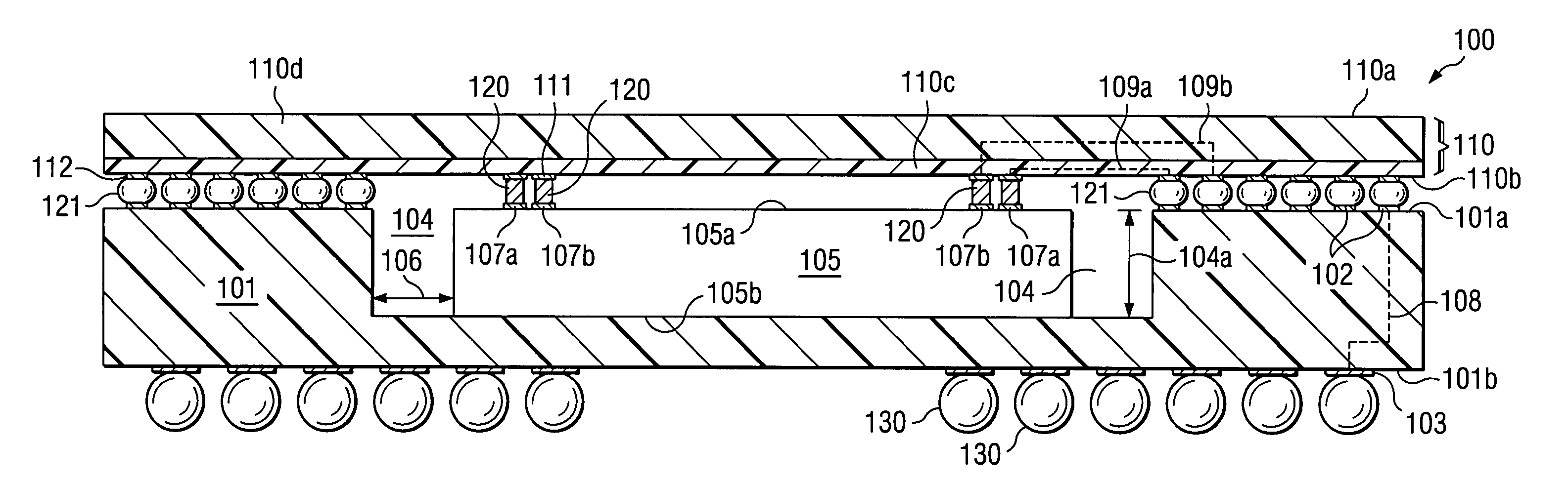
[0019] The schematic cross section of FIG. 1 illustrates a packaged integrated circuit (IC) device for enhanced speed and power performance, generally designated 100, representing an embodiment of the invention. The package comprises a first package part 101 made of plastic, including FR-4, or ceramic, which has a top surface 101a and a bottom surface 101b. On top surface 101a is a plurality of I / O terminal pads 102, and on bottom surface 101b is another plurality of I / O terminals pads 103. Integral with package part 101 are connector lines between terminal pads 102 and terminal pads 103; an example of these connector lines is schematically shown in FIG. 1 as dashed trace 108.

[0020] The first package part 101 is formed so that it offers a cavity 104, which is shaped to have an integrated circuit chip 105 mounted in cavity 104. It is a technical advantage of this embodiment of the invention that cavity 104 is sized so that it can accept a variety of chip sizes 105. Chips 105 may hav...


PUM


Abstract

An integrated circuit device package with a first part (101) having a cavity (104) to mount the chip (105), further I/O terminals (102) on the top surface and terminals (103) on the bottom surface. The chip has contact pads (107a and 107b). The second part (110) of the package has bottom surface terminals (111) aligned with the chip contact pads, and bottom terminals (112) aligned with the terminals (102) of the first package part. The connections are provided by stud bumps between the chip contact pads and terminals (111), and by reflow material between terminals (102) and (112). The connector lines (109a and 109b) in the second package part (110) comprise signal/power and ground layers. The layers are spaced by insulation between, 10 and 50 μm thick, and the connector lines have a width less than three times the insulator thickness.

Description

FIELD OF THE INVENTION [0001] The present invention is related in general to the field of semiconductor devices and more specifically to structures and fabrication methods of ball grid array packages providing for increased input / output terminals, speed and power. DESCRIPTION OF THE RELATED ART [0002] Two of the ongoing trends in integrated circuit (IC) technology, are the drives towards higher integration and shrinking component feature sizes. Higher levels of integration include the need for higher numbers of signal lines and power lines, yet smaller feature sizes make it more and more difficult to preserve clean signals without mutual interference. In addition, with increasing signal frequencies, transmission and shielding of signals require careful attention. [0003] These trends and requirements do not only dominate the semiconductor chips, which incorporate the ICs, but also the packages, which house and protect the IC chips. Actually, boards and other parts of an electronic pr...

Claims


Application Information

Patent Timeline
Patent Type & Authority Applications(United States)
IPC IPC(8): H01L23/13H01L23/498
CPCH01L23/13H01L2924/15192H01L23/49833H01L24/73H01L2224/48091H01L2224/4824H01L2224/48465H01L2224/49175H01L2224/73207H01L2924/01029H01L2924/01032H01L2924/01046H01L2924/01049H01L2924/01077H01L2924/01078H01L2924/01079H01L2924/01082H01L2924/14H01L2924/15153H01L2924/15165H01L2924/15311H01L2924/30107H01L2924/3011H01L2924/3025H01L23/49816H01L2224/73253H01L2224/32225H01L2224/16225H01L2224/45144H01L2924/01087H01L2924/01076H01L2924/01047H01L2924/01033H01L2924/01005H01L24/49H01L24/48H01L2924/00014H01L2924/00H01L24/45H01L2224/05568H01L2224/05573H01L2924/15321H01L2924/181H01L2924/00015H01L2224/05599
Inventor HOWARD, GREGORY E.SARAN, MUKUL
Owner TEXAS INSTR INC
Why Eureka
Try Eureka