Liquid crystal display device and fabrication method thereof

Inactive Publication Date: 2005-01-13
HITACHI LTD
8 Cites 47 Cited by

AI-Extracted Technical Summary

Problems solved by technology

Moreover, in Japanese Patent Laid-Open No. 232409/1998, although the TFT glass substrate of a lateral electric field type, i.e., the IPS display mode, of liquid crystal display device is formed through four photo-processes, the terminals of its gate and drain wiring lines are not coated with a transparent conductive film such as Indium-Tin-Oxide (hereinafter, ITO), so that the terminals suffer the problem of electrical corrosion due to humidity.
In addition, s...

Method used

[0105] In the TFT section of the liquid crystal display device, as shown in FIG. 2 in cross section, a gate wiring line GL made of a metal film g1 in which, for example, Mo (molybdenum) is stacked on Mo, Cr (chromium) or Al (aluminum) is formed on a transparent insulating substrate SUB1 such as a glass substrate. An a-Si channel film AS using i-type a-Si is formed over this gate wiring line GL with a gate insulating film GI interposed therebetween, where the gate insulating film GI is made of an SiN film or a stacked film composed of an SiO2 film and an SiN film. Furthermore, a drain electrode SD1 and a source electrode SD2 each made of Mo, Cr or a stacked layer of Mo, Al and Mo are formed over this a-Si channel film AS on both sides thereof in the state of being opposite to each other with a contact film d0 using an n+-type a-Si film being interposed between the a-Si channel film AS and the drain electrode SD1 as well as between the a-Si channel film AS and the source electrode SD2. This drain electrode SD1 constitutes part of the video signal line DL. The a-Si contact layer d0 and the a-Si channel film AS are partly removed by etching from above the portion between the drain electrode and the source electrode in order to increase the off resistance of TFT operation, whereby the thickness of the a-Si channel film AS in this region is set to be smaller than the thickness of the a-Si channel film AS excluding the a-Si contact layer d0 lying under the drain electrode SD1 and the source electrode SD2. Moreover, a contact hole CN is formed in a protective film PSV made of an SiN film covering the TFT, and a transparent conductive film ITO1 made of ITO is connected to the source electrode SD2 through the contact hole CN and constitutes the pixel electrode PX.
[0108] As shown in FIGS. 1 and 3, the signal line DL has the function of mainly transmitting a video signal voltage, and is composed of the metal film d1 made of a Mo—Cr alloy or a stacked layer in which Mo, Al and Mo are stacked in this order, and the a-Si contact films d0 and AS. The cross-sectional structure of the signal line DL has a staircase-like shape similar to the source electrode SD2, and the a-Si channel film AS projects from the metal film d1. Light shielding electrodes SKD which are formed of the same material as and in the same step as the gate wiring line GL are disposed below both sides of the video signal line DL, respectively. The light shielding electrodes SKD have the effect of blocking the gap between the pixel electrode PX and the video signal line DL, and is capable of narrowing the width of a black matrix BM made of a metal or a resin of low optical transmissivity formed on a color filter substrate SUB2 which is a substrate disposed to be opposite to the TFT substrate SUB1 across a liquid crystal LC interposed between alignment films ORI. In this manner, the light shielding electrodes SKD makes it possible to increase the aperture ratio, thereby realizing a bright liquid crystal display device (having a pixel with high optical transmissivity). In FIG. 3, symbol FIL denotes a color filter, and symbol CX denotes a counter (common) electrode using an electrode IT02 made of a transparent conductive film such as ITO. Polarizer films POL are fitted to the outer surfaces of the respective TFT substrates SUB1 and SUB2.
[0115] As shown in FIGS. 1 and 5, a terminal section DTM of the drain wiring line DL has a structure in which the metal film d1, the a-Si contact film d0 and the a-Si channel film AS are formed in a staircase-like shape similar to that of the video signal line DL, and the protective film PSV for the TFT is formed over the films d1, d0 an AS, and the transparent conductive film ITO1 which is made of the same material as the pixel electrode PX formed on the protective film PSV is formed on the metal film via a through-hole formed in the protective film PSV. In this structure, the a-Si contact film d0 and the a-Si channel film AS which are semiconductor films acts to improve the adherence between the metal film d1 and the gate insulating film GI both of which use, for example, Mo. The display-area sides of the gate terminals GTM and the drain terminals DTM are respectively supplied with the voltages required to be supplied to the gate wiring lines GL and the video signal lines DL for the purpose of displaying, and the gate terminals GTM and the drain terminals DTM are connected to external control circuits.
[0118] A second photo-process is shown in FIGS. 7A to 7D. A 350-nm-thick insulating film which is made of a SiN film or a two-layer film made of an SiN film and a SiO2 film, a 250-nm-thick nondoped i-type a-Si film and a 50-nm-thick n+-type a-Si film are deposited in that order over the entire surface of the TFT substrate SUB1 by using a plasma CVD method. The SiN film, the i-type a-Si film and the n+-type a-Si film are respectively called the gate insulating film GI, the a-Si channel film AS and the a-Si contact film d0 in terms of TFT construction. However, although the gate insulating film GI is formed by the CVD method, the gate insulating film GI may also be formed as a multilayer structure by depositing a metal oxide such as Ta2O5 (tantalum oxide) by using a sputtering method before the CVD method. Subsequently, a 200-nm-thick metal film d1 such as a single Mo or Cr SiN film, a Mo/Al/Mo stacked film or an alloy film such as MoW is deposited by using the sputtering method. The deposition by the CVD method and the deposition by the sputtering method may also be continuously performed without breaking the vacuum. In this case, the connection resistance between the a-Si contact film d0 and the Mo metal film d1 which constitutes the source and drain electrodes is reduced and the capacity of TFTs is improved, whereby even if TFTs of the same plane size are used, it is possible to drive a larger-sized and higher-resolution liquid crystal display device. In addition, since the nontransparent TFT area which occupies the plane area of one pixel can be reduced, the aperture ratio is improved, whereby it is possible to provide a far brighter liquid crystal display device.
[0119] Then, a predetermined resist pattern (photo-resist pattern) is formed on this metal film dl. In FIG. 7A, the resist pattern PRES1 and a resist pattern PRES2 form resist pattern areas having different thicknesses through one exposure and development process. Such a resist pattern having a thick region and a thin region is obtained through so-called half-exposure process. The half-exposure process exposes a predetermined portion of a photo-resist layer so weakly that exposing depth of the predetermined region thereof does not to reach the thickness thereof and the predetermined portion thereof remains as the aforementioned thin region in contrast to the other region thereof being not exposed and remaining as the aforementioned thick region. The process of forming the resist patterns of different thicknesses through one exposure and development process reduces the number of fabrication processes for TFT substrates and realizes an improvement in yield factor. A method of fabricating such different resist patterns will be described below with reference to the photomask substrate MASUB shown in FIG. 7A.
[0121] The photomask fabrication method which forms resist patterns of different thicknesses on the TFT substrate SUB1 through one exposure and development process is not limited to the above-described method of forming the semitransparent metal area MAK2, but as disclosed in Japanese Patent Laid-Open No. 186233/1997, it is also possible to use a halftone mask in which the area MAK2 is made of a mesh-formed metal film having the same thickness as the area MAK1 so that the amount of exposure of the resist is reduced. However, as compared with the method of Embodiment 1, the method using such a halftone is low in the margin for adjustment of the amount of exposure reduction.
[0124] Then, the metal film d1 and the i-type a-Si channel film AS are half-etched so that a predetermined thickness is left, by using as a mask the resist pattern PRES1 which has been divided into sections corresponding to the source and drain electrode SD1 and SD2. In this process, the metal film d0 is removed by wet etching, and the etch selectivity of the a-Si contact layer do relative to SiN is increased by adjusting the amount of Cl2 to be added to SF6 or CF4.
[0125] As described above, as compared with the prior art of performing the processing of an a-Si film and the processing of source and drain metals through two separate photo-processes, it is possible to integrate these processes into one process by using the semitransparent mask, whereby it is possible to realize a reduction in the number of required fabrication processes and hence an improvement in yield factor. In addition, since there is no need for photo-alignment of the a-Si film and the source and drain metal films, accuracy is improved and aperture ratio is also improved.
[0126] On the other hand, as compared with the prior art method, the metal films for the source and drain electrodes SD1 and SD2 as well as the drain wiring line DL are etched twice, and if the metal film d1 is wet-etched, the amount of undercutting due to side etching becomes large and pattern accuracy becomes low. On the other hand, dry etching features a high pattern accuracy, but in the second etching (channel length L portion) shown in FIG. 7D, if the wiring metals contain Mo, the same kind of etching gas as that for the the a-Si channel film AS at the lower portion is used and, in addition, processing is performed so that the thickness of the a-Si channel film AS is reduced to half. If the a-Si channel film AS is etched in batch, the margin of etching cannot be ensured and the channel length L area is removed up to the surface of the gate insulating film GI. In the case of Embodiment 1, if the metal film d1 contains Mo, the channel length portion of the metal film d1 is selectively wet-etched above the a-Si film d0 by using a mixture of phosphoric acid, nitric acid, acetic acid and water, and then, the a-Si film d0 is dry-etched, whereby the process is controlled so that the a-Si channel-film AS is left. Consequently, it is found out that the method of subjecting the metal film d1 for the source and drain electrodes SD1 and SD2 to dry etching as the first etching and wet etching as the second etching within one photo-process realizes a processing method of good pattern accuracy.
[0129] In accordance with the above-described fabrication process of Embodiment 1, as compared with the prior art fabrication process, it is possible to reduce the number of required photo-processes including exposure and development from five to four, whereby it is possible to simplify the fabrication process and it is also possible to reduce defects due to dust or the like occurring in a process and improve the yield factor of the fabrication process. In addition, in terms of the TFT structure, the a-Si film and the signal lines are processed in one photo-process after having been continuously deposited, whereby the pattern accuracy of Embodiment 1 is improved compared to the conventional pattern accuracy with which a-Si films, signal lines and source and drain electrodes are separately processed through photo-alignment. Accordingly, it is possible to realize a bright liquid crystal display device having a high aperture ratio.
[0138] The charge-holding capacitance Cstg of Embodiment 2 has a laminated structure consisting of an upper electrode made of the transparent conductive film ITO1 which is formed in the same process and of the same material as the pixel electrode PX and a lower electrode which is the gate wiring line GL, as in Embodiment 1. However, unlike the charge-holding capacitance Cstg of Embodiment 1, the charge-holding capacitance Cstg of Embodiment 2 has a dielectric film having a stacked structure made of the SiN gate insulating film GI and the half-etched a-Si channel film AS. In the structure of the charge-holding capacitance Cstg of Embodiment 2, the dielectric film is thin in thickness compared to the dielectric film of Embodiment 1 having a stacked structure made of the SiN gate wiring line GL and the SiN protective film. Moreover, the dielectric constant of the a-Si film is 12 which is greater than 7 of the SiN film, whereby Embodiment 2 makes it possible to form a larger charge-holding capacitance Cstg in a smaller area than does Embodiment 1. Accordingly, since the width of the gate wiring line GL can be made narrower in Embodiment 2 shown in FIG. 10 than in Embodiment 1 shown in FIG. 1, the aperture ratio can be increased, whereby it is possible to realize a bright liquid crystal display device.
[0140] As compared with the above-described prior art, in Embodiment 2, the image retention is reduced owing to the following advantages, whereby it is possible to realize a good display device. One of the advantages is that the a-Si channel film AS of the charge-holding capacitance Cstg shown in FIG. 11 is thinned by half-etching after deposition, and the second one is that in the structure of Embodiment 2 the a-Si contact film d0 is removed and the efficiency of injection of electrons into the a-Si channel film AS from the transparent conductive film ITO1 of the pixel electrode PX is extremely small (the contact resistance is large). Accordingly, in the structure of Embodiment 2, the a-Si channel film AS purely works as a dielectric, whereby it is possible to realize a good liquid crystal display device in which no image retention occurs.
[0146] Then, the a-Si channel film AS over the charge-holding capacitance Cstg is selectively etched above the gate insulating film GI formed of SiN at the opening CNS with the resist pattern PRES1 being left. The etching is performed with a so-called chlorine type gas in which Cl2 or HCl is added to SF6 or CF4. If the outermost surface of the metal film d1 of the source electrode SD2 is made of Cr or a metal containing Cr, the a-Si channel film AS is not removed by the dry etching using the chlorine gas. If the outermost surface is made of Mo or a metal which mainly contains Mo, the speed of the drying etching for the processing of the through-holes is slower than that for the a-Si channel film AS in the section of the charge-holding capacitance Cstg. Accordingly, the metal film dl of the source electrode SD2 is not completely removed when the etching of the a-Si channel film AS is completed, whereby it is possible to achieve the good contact characteristics between the source electrode SD2 and the transparent conductive film ITO1. The favorable effect of the above-described etching is also achieved due to t...

Benefits of technology

[0070] By using a photomask having three areas having different optical transmissivities, it is possible to process drain wiring lines, source electrodes and drain electrodes and s-Si films through one photo-process for exposure and development, whereby it is possible to simplify the entire process. In addition, the number of photo-processes per TFT ...

Abstract

The present invention provides a novel photolithography processes using photoresist pattern having at least two areas which has different thickness from each other for a fabrication method for a liquid crystal display device having reversed staggered and channel-etched type thin film transistors, reduce a number of photolithography processes required for whole of the fabrication process of the liquid crystal display device, and improve brightness of the liquid crystal display device.

Application Domain

Technology Topic

Image

  • Liquid crystal display device and fabrication method thereof
  • Liquid crystal display device and fabrication method thereof
  • Liquid crystal display device and fabrication method thereof

Examples

  • Experimental program(7)

Example

[0104]FIG. 1 is a plan view showing a TFT substrate of a type according to Embodiment 1 of the invention. FIG. 2 is a cross-sectional view taken along line 2-2 of FIG. 1, showing a portion which extends from a TFT to a charge-holding capacitance portion Cstg through a pixel electrode PX. FIG. 3 is a cross-sectional view taken along line 3-3 of FIG. 1, showing a drain wiring line section. FIG. 4 is a cross-sectional view taken along line 4-4 of FIG. 1, showing a gate wiring line section. FIG. 5 is a cross-sectional view taken along line 5-5 of FIG. 1, showing a drain wiring line section. FIGS. 6A to 9B are cross-sectional views showing a fabrication method for the TFT substrate according to Embodiment 1 in the order of steps (from photoresist application to resist stripping) of a photo-process which is basically patterning, the respective steps corresponding to FIGS. 6A and 6B; 7A to 7D; 8A and 8B; and 9A and 9B.
[0105] In the TFT section of the liquid crystal display device, as shown in FIG. 2 in cross section, a gate wiring line GL made of a metal film g1 in which, for example, Mo (molybdenum) is stacked on Mo, Cr (chromium) or Al (aluminum) is formed on a transparent insulating substrate SUB1 such as a glass substrate. An a-Si channel film AS using i-type a-Si is formed over this gate wiring line GL with a gate insulating film GI interposed therebetween, where the gate insulating film GI is made of an SiN film or a stacked film composed of an SiO2 film and an SiN film. Furthermore, a drain electrode SD1 and a source electrode SD2 each made of Mo, Cr or a stacked layer of Mo, Al and Mo are formed over this a-Si channel film AS on both sides thereof in the state of being opposite to each other with a contact film d0 using an n+-type a-Si film being interposed between the a-Si channel film AS and the drain electrode SD1 as well as between the a-Si channel film AS and the source electrode SD2. This drain electrode SD1 constitutes part of the video signal line DL. The a-Si contact layer d0 and the a-Si channel film AS are partly removed by etching from above the portion between the drain electrode and the source electrode in order to increase the off resistance of TFT operation, whereby the thickness of the a-Si channel film AS in this region is set to be smaller than the thickness of the a-Si channel film AS excluding the a-Si contact layer d0 lying under the drain electrode SD1 and the source electrode SD2. Moreover, a contact hole CN is formed in a protective film PSV made of an SiN film covering the TFT, and a transparent conductive film ITO1 made of ITO is connected to the source electrode SD2 through the contact hole CN and constitutes the pixel electrode PX.
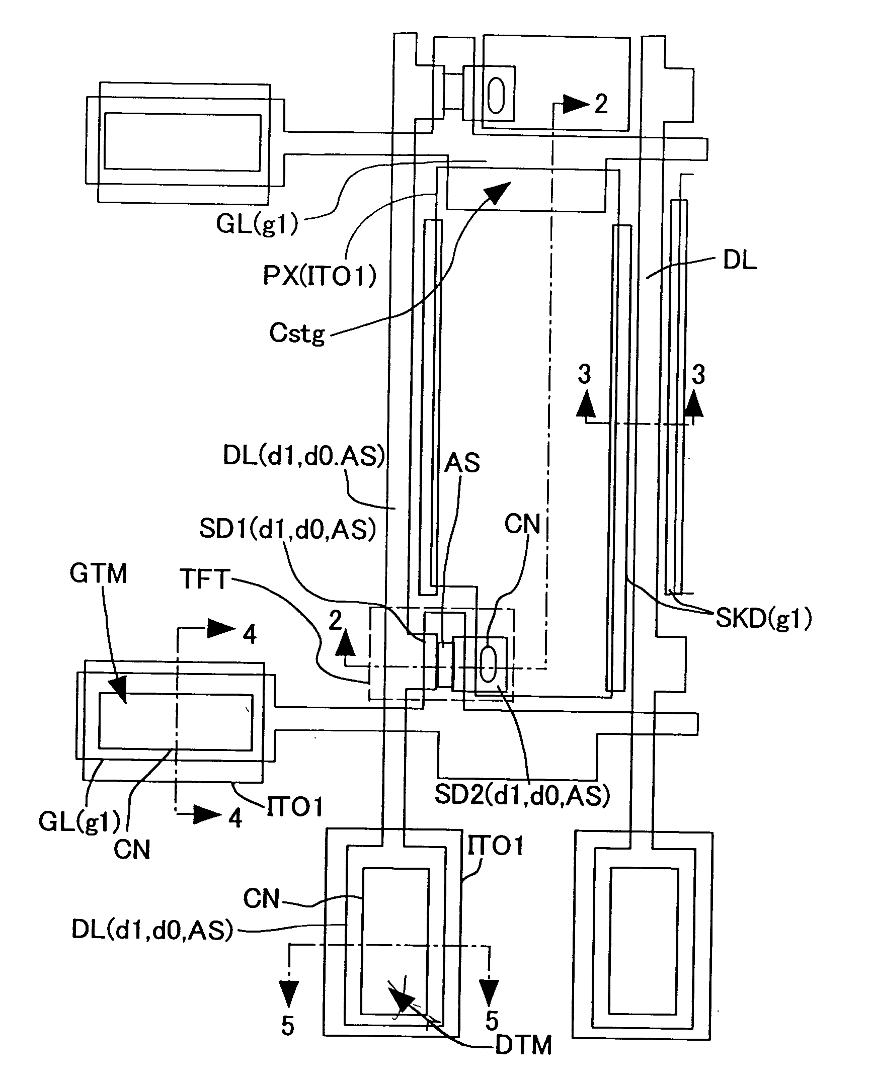
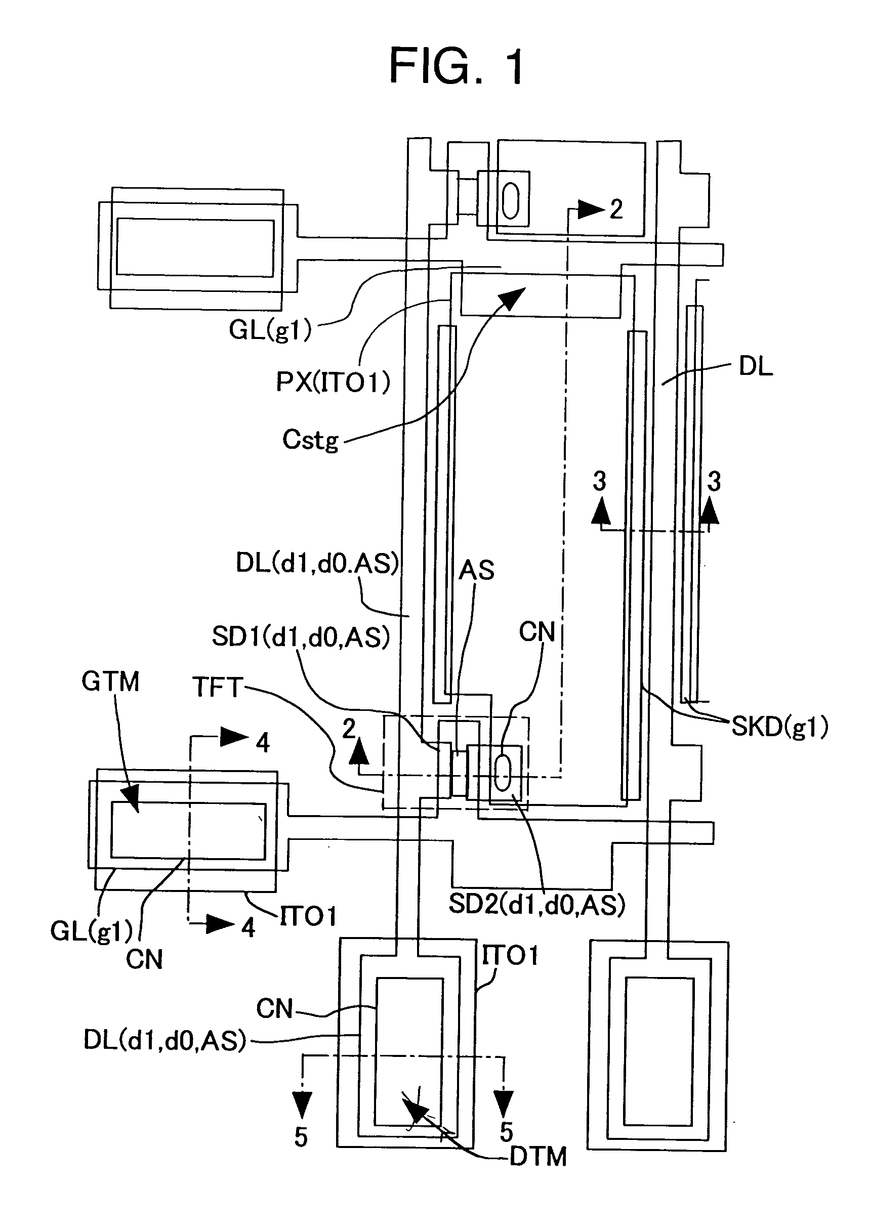
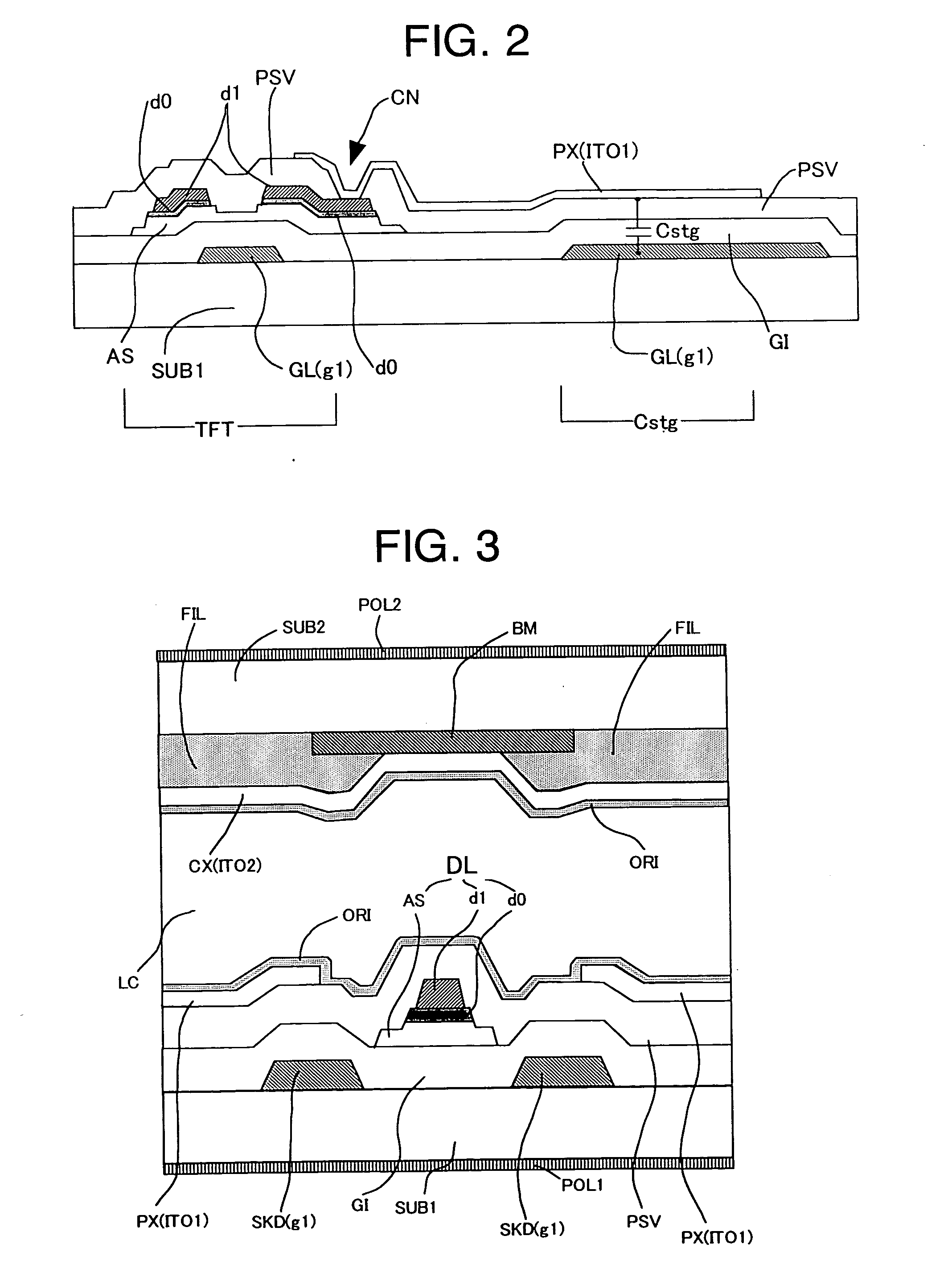
[0106] In the construction of this TFT section, one problem to be solved in terms of manufacturing yield factor is that the material of the transparent conductive film ITO1 which constitutes the pixel electrode PX, for example, ITO, does not have sufficient adhesion to the stepped undersurface, so that the transparent conductive film ITO1 may be easily disconnected during etching processing. Particularly in the cross-sectional structure shown in FIG. 2, the source electrode SD2 that lies near the contact hole CN has a large stepped interval because the a-Si films AS and d0 and the metal electrode d0 are stacked. In Embodiment 1, the a-Si contact film d0 projects from an overlying metal material d1 which constitutes the drain electrode SD1, and the a-Si channel film AS projects from the overlying a-Si contact film d0. The resultant steps constitute a staircase-like structure which is formed by the metal material d1, a semiconductor film including the a-Si contact film d0, and the portion of the a-Si channel film AS that is made thin by etching. The protective film PSV which is formed over the staircase-like structure has a gentle shape so that the transparent conductive film ITO1 is not at all disconnected.
[0107] In the section of the charge-holding capacitance Cstg, as shown in FIGS. 1 and 2, the pixel electrode PX made of the transparent conductive film ITO1 is extended to overlap the adjacent gate wiring line GL. Therefore, the charge-holding capacitance Cstg has an upper electrode made of the transparent conductive film ITO1 which constitutes the pixel electrode PX, a lower electrode made of the electrode g1 which constitutes the gate wiring line GL, and a dielectric film having a stacked structure made of the gate insulating film GI and the protective film PSV.
[0108] As shown in FIGS. 1 and 3, the signal line DL has the function of mainly transmitting a video signal voltage, and is composed of the metal film d1 made of a Mo—Cr alloy or a stacked layer in which Mo, Al and Mo are stacked in this order, and the a-Si contact films d0 and AS. The cross-sectional structure of the signal line DL has a staircase-like shape similar to the source electrode SD2, and the a-Si channel film AS projects from the metal film d1. Light shielding electrodes SKD which are formed of the same material as and in the same step as the gate wiring line GL are disposed below both sides of the video signal line DL, respectively. The light shielding electrodes SKD have the effect of blocking the gap between the pixel electrode PX and the video signal line DL, and is capable of narrowing the width of a black matrix BM made of a metal or a resin of low optical transmissivity formed on a color filter substrate SUB2 which is a substrate disposed to be opposite to the TFT substrate SUB1 across a liquid crystal LC interposed between alignment films ORI. In this manner, the light shielding electrodes SKD makes it possible to increase the aperture ratio, thereby realizing a bright liquid crystal display device (having a pixel with high optical transmissivity). In FIG. 3, symbol FIL denotes a color filter, and symbol CX denotes a counter (common) electrode using an electrode IT02 made of a transparent conductive film such as ITO. Polarizer films POL are fitted to the outer surfaces of the respective TFT substrates SUB1 and SUB2.
[0109] The following effects are obtained from the structure of the video signal line DL which is not simply made of the metal film d1 alone but has staircase-like steps made of the metal film d1, the a-Si contact film d0 and the a-Si channel film AS, respectively. As the metal film d1, Cr can also be used, but Al or Mo is preferable as a material of low resistivity.
[0110] However, during the etching of the transparent conductive film ITO1 of the pixel electrode PX which is located at the top of the cross-sectional structure shown in FIG. 3, Al is easily dissolved through a pinhole in the protective film PSV by an aqueous solution of HBr or Hl which is an etching chemical, thus resulting in disconnection. For this reason, in the case where the resistivity of CR does not suffice, either a single MO film resistant to the etching chemical or a wiring metal structure in which an Al layer is sandwiched between upper and lower Mo layers is selected. On the other hand, Mo does not have good adhesion to an insulating film. Since Mo has high adherence to an a-Si film because Mo and the a-Si film form silicide, the a-Si contact film d0 which is a semiconductor is formed under the metal film d1. On the other hand, in the case where the films d0 and AS which are semiconductor films are deposited by an apparatus different from that for the metal film d1 and are processed by using a so-called photo-process, if the semiconductor films d0 and AS and the metal film d1 are subjected to different photo-processes, the width of the structure of the video signal line DL becomes large due to a deviation in alignment between the photo-processes, so that the aperture ratio decreases, resulting in a dark liquid crystal display device. Moreover, at the time of the rubbing of the upper portion of the alignment film ORI as viewed in FIG. 3, a structure having gentle steps is needed. As a result, it is preferable that the steps formed by the metal film d1, the a-Si contact film d0 and the a-Si channel film AS constitute a staircase-like structure, and in terms of a fabrication method, as will be described later in detail, it is preferable to continuously deposit the a-Si channel film AS, the a-Si contact film d0 and the source and drain metal film d1 and process these films from above by a single photoresist process.
[0111] In Embodiment 1, this method is used.
[0112] Another problem to be solved in terms of manufacturing yield factor is the disconnection of the video signal line DL which intersects a plurality of gate wiring lines GL as shown in FIG. 1. Such disconnection will be described with reference to the cross-sectional view of FIG. 2. A material such as Cr or Mo is used for the metal film D1 which constitutes the video signal line DL (the drain electrode SD1). Depending on deposition conditions, tensile stress occurs in such material.
[0113] Since the video signal line DL is tensed in its lengthwise direction (in a direction perpendicular to the extending direction of the gate wiring lines GL; refer to FIG. 1), the video signal line DL is disconnected at any of the steps of the underling gate wiring lines GL. On the other hand, the i-type a-Si film AS has compressive stress, so that if the a-Si film AS is formed under the metal film d1 which constitutes the video signal line DL, the stress is relaxed. Moreover, since the stress of the metal film d1 is on the same order as the stress of the a-Si channel film AS, the width of the a-Si channel film AS is preferably made equal to or slightly larger than the width of the metal film dl.
[0114] As shown in FIGS. 1 and 4, a terminal section GTM of the gate wiring line GL has a structure in which a lower gate terminal electrode is made of the electrode g1 which constitutes a film common to the gate wiring line GL formed on the TFT substrate SUB1, and the gate insulating film GI and the protective film PSV are formed over the electrode g1, and an upper gate terminal electrode which is made of the transparent conductive film ITO1 of the same material as the pixel electrode PX is stacked on the electrode g1 via a through-hole formed in the stacked film made of the films GI and PSV.
[0115] As shown in FIGS. 1 and 5, a terminal section DTM of the drain wiring line DL has a structure in which the metal film d1, the a-Si contact film d0 and the a-Si channel film AS are formed in a staircase-like shape similar to that of the video signal line DL, and the protective film PSV for the TFT is formed over the films d1, d0 an AS, and the transparent conductive film ITO1 which is made of the same material as the pixel electrode PX formed on the protective film PSV is formed on the metal film via a through-hole formed in the protective film PSV. In this structure, the a-Si contact film d0 and the a-Si channel film AS which are semiconductor films acts to improve the adherence between the metal film d1 and the gate insulating film GI both of which use, for example, Mo. The display-area sides of the gate terminals GTM and the drain terminals DTM are respectively supplied with the voltages required to be supplied to the gate wiring lines GL and the video signal lines DL for the purpose of displaying, and the gate terminals GTM and the drain terminals DTM are connected to external control circuits.
[0116] A fabrication method for the TFT substrate of the reversed staggered type TFT display device shown in FIG. 2 will be described below with reference to the cross-sectional process diagrams of FIGS. 6A to 9B. Each sheet of FIGS. 6A to 9B approximately corresponds to one photo-process, and processes which are basically photo-patterning, i.e., thin film deposition, photoresist application, exposure, development and thin film patterning, will be described below as one photo-process. The illustration of a photoresist stripping step is omitted in FIGS. 6A to 9B. The detailed procedures of each photo-process are represented by the cross-sectional views of the corresponding FIGS. 6A to 9B.
[0117] A first photo-process is shown in FIGS. 6A and 6B. A 200-nm-thick metal film g1, which is made of, for example, a single Cr or Mo film or a stacked film in which Al and Mo are stacked in this order or an alloy such as MoW, is deposited on a transparent insulating substrate SUB1 such as a glass substrate by using a sputtering method. Then, after a predetermined resist pattern PRES1 has been formed on this metal film g1, the metal film g1 is etched by using the predetermined resist pattern PRES1 as a mask. This patterned metal film g1 constitutes the gate wiring lines GL, the light shielding electrodes SKD and the lower electrodes of the gate terminals GTM in the pixel area shown in FIG. 1.
[0118] A second photo-process is shown in FIGS. 7A to 7D. A 350-nm-thick insulating film which is made of a SiN film or a two-layer film made of an SiN film and a SiO2 film, a 250-nm-thick nondoped i-type a-Si film and a 50-nm-thick n+-type a-Si film are deposited in that order over the entire surface of the TFT substrate SUB1 by using a plasma CVD method. The SiN film, the i-type a-Si film and the n+-type a-Si film are respectively called the gate insulating film GI, the a-Si channel film AS and the a-Si contact film d0 in terms of TFT construction. However, although the gate insulating film GI is formed by the CVD method, the gate insulating film GI may also be formed as a multilayer structure by depositing a metal oxide such as Ta2O5 (tantalum oxide) by using a sputtering method before the CVD method. Subsequently, a 200-nm-thick metal film d1 such as a single Mo or Cr SiN film, a Mo/Al/Mo stacked film or an alloy film such as MoW is deposited by using the sputtering method. The deposition by the CVD method and the deposition by the sputtering method may also be continuously performed without breaking the vacuum. In this case, the connection resistance between the a-Si contact film d0 and the Mo metal film d1 which constitutes the source and drain electrodes is reduced and the capacity of TFTs is improved, whereby even if TFTs of the same plane size are used, it is possible to drive a larger-sized and higher-resolution liquid crystal display device. In addition, since the nontransparent TFT area which occupies the plane area of one pixel can be reduced, the aperture ratio is improved, whereby it is possible to provide a far brighter liquid crystal display device.
[0119] Then, a predetermined resist pattern (photo-resist pattern) is formed on this metal film dl. In FIG. 7A, the resist pattern PRES1 and a resist pattern PRES2 form resist pattern areas having different thicknesses through one exposure and development process. Such a resist pattern having a thick region and a thin region is obtained through so-called half-exposure process. The half-exposure process exposes a predetermined portion of a photo-resist layer so weakly that exposing depth of the predetermined region thereof does not to reach the thickness thereof and the predetermined portion thereof remains as the aforementioned thin region in contrast to the other region thereof being not exposed and remaining as the aforementioned thick region. The process of forming the resist patterns of different thicknesses through one exposure and development process reduces the number of fabrication processes for TFT substrates and realizes an improvement in yield factor. A method of fabricating such different resist patterns will be described below with reference to the photomask substrate MASUB shown in FIG. 7A.
[0120] In the photo-process, the photomask is disposed over the TFT substrate SUB1 whose entire surface is coated with a resist, with a predetermined gap interposed between the photomask and the TFT substrate SUB1. The photomask has a structure having a nontransparent area (an opaque area) MAK1 made of Cr deposited to a predetermined thickness, an area MAK2 made of thinly deposited MoSi which can transmit light to a predetermined degree, and the other transparent area. In the case where a positive resist is used as the resist, the thickness of the resist after exposure and development becomes approximately close to the thickness of deposited film in the nontransparent area MAK1, and to a thickness 10-90% less than the thickness of film being deposited in the semitransparent area MAK2, and in the other transparent areas the resist is completely removed by cleaning. Accordingly, since the pattern of the photomask substrate MASUB is formed into three areas, i.e., nontransparent, semitransparent and transparent, the resist patterns PRES1 and PRES2 of different thicknesses can be realized on the TFT substrate SUB1 through one exposure and development process. In the next process et seq., the area of the resist pattern PRES1 forms the video signal lines DL for TFTs as well as the source and drain electrodes SD1 and SD2, while the area of the resist pattern PRES2 forms the channel length L areas of the TFTs.
[0121] The photomask fabrication method which forms resist patterns of different thicknesses on the TFT substrate SUB1 through one exposure and development process is not limited to the above-described method of forming the semitransparent metal area MAK2, but as disclosed in Japanese Patent Laid-Open No. 186233/1997, it is also possible to use a halftone mask in which the area MAK2 is made of a mesh-formed metal film having the same thickness as the area MAK1 so that the amount of exposure of the resist is reduced. However, as compared with the method of Embodiment 1, the method using such a halftone is low in the margin for adjustment of the amount of exposure reduction.
[0122] Then, as shown in the next cross-sectional view of the photo-process (FIG. 7B), the metal film d1, the a-Si contact film d0 and the a-Si channel film AS are etched by using a predetermined resist pattern on the metal film d1 as a mask. The etching is performed with dry etching in a vacuum apparatus, and if the metal film d1 is Mo, etching is performed with a gas in which O2 is added to a SF6 or CC14 gas, or with this gas to which Cl2 is further added, and the semiconductor films d0 and AS are etched with a gas in which HCl or Cl2 is added to a gas containing at least SF6 or CF4 so that the etch selectivity of the semiconductor films d0 and AS is increased with respect to SiN which is the material of the gate insulating film GI. As described above, by dry-etching the metal film d1 for the source and drain electrodes SD1 and SD2 as well as the semiconductor films d0 and AS, the pattern accuracy of the video signal line DL formed by processing these films d1, d0 and AS can be made extremely high.
[0123] Then, as shown in FIG. 7C, dry ashing using an O2 gas is used to remove a thin resist pattern which lies in the channel length L area of the TFT. During this time, although the thickness of the thick resist pattern PRES1 decreases, ashing conditions are adjusted so that the resist pattern PRES1 can be left as a photoresist pattern.
[0124] Then, the metal film d1 and the i-type a-Si channel film AS are half-etched so that a predetermined thickness is left, by using as a mask the resist pattern PRES1 which has been divided into sections corresponding to the source and drain electrode SD1 and SD2. In this process, the metal film d0 is removed by wet etching, and the etch selectivity of the a-Si contact layer do relative to SiN is increased by adjusting the amount of Cl2 to be added to SF6 or CF4.
[0125] As described above, as compared with the prior art of performing the processing of an a-Si film and the processing of source and drain metals through two separate photo-processes, it is possible to integrate these processes into one process by using the semitransparent mask, whereby it is possible to realize a reduction in the number of required fabrication processes and hence an improvement in yield factor. In addition, since there is no need for photo-alignment of the a-Si film and the source and drain metal films, accuracy is improved and aperture ratio is also improved.
[0126] On the other hand, as compared with the prior art method, the metal films for the source and drain electrodes SD1 and SD2 as well as the drain wiring line DL are etched twice, and if the metal film d1 is wet-etched, the amount of undercutting due to side etching becomes large and pattern accuracy becomes low. On the other hand, dry etching features a high pattern accuracy, but in the second etching (channel length L portion) shown in FIG. 7D, if the wiring metals contain Mo, the same kind of etching gas as that for the the a-Si channel film AS at the lower portion is used and, in addition, processing is performed so that the thickness of the a-Si channel film AS is reduced to half. If the a-Si channel film AS is etched in batch, the margin of etching cannot be ensured and the channel length L area is removed up to the surface of the gate insulating film GI. In the case of Embodiment 1, if the metal film d1 contains Mo, the channel length portion of the metal film d1 is selectively wet-etched above the a-Si film d0 by using a mixture of phosphoric acid, nitric acid, acetic acid and water, and then, the a-Si film d0 is dry-etched, whereby the process is controlled so that the a-Si channel-film AS is left. Consequently, it is found out that the method of subjecting the metal film d1 for the source and drain electrodes SD1 and SD2 to dry etching as the first etching and wet etching as the second etching within one photo-process realizes a processing method of good pattern accuracy.
[0127] Alternative photo-processes for the TFT substrate are shown in FIGS. 8A to 9B. A 400-nm-thick protective film PSV made of an SiN film is deposited on the entire surface of the TFT substrate SUB1 which has passed through the above-described process, by using a CVD method. Then, after a resist has been applied to the protective film PSV, a resist pattern PRES1 having an opening above the source electrode SD2 is formed by using a photo-method. Then, the contact hole CN is formed in the protective film PSV by using the resist pattern PRES1 as a mask. In this process, the gate terminal GTM and the drain terminal DTM shown in FIG. 1 are also processed, and as shown in FIG. 4, the laminated protective film PSV and the gate insulating film GI are opened at the gate terminal GTM in this process. The formation of this opening uses dry etching using a gas containing SF6 or CF4 or wet etching using a buffer solution of hydrofluoric acid.
[0128] Then, as shown in FIGS. 9A and 9B, a 140-nm-thick transparent conductive film ITO1 made of ITO or IZO is deposited on the entire surface of the TFT substrate SUB1 by using a sputtering method. Then, after a resist pattern PRES1 is formed, this transparent conductive film ITO1 is processed by using the resist pattern PRES1 as a mask, thereby forming the pixel electrode PX. In addition, in this process, the upper film ITO1 of each of the terminal sections shown in FIGS. 1, 4 and 5 is formed.
[0129] In accordance with the above-described fabrication process of Embodiment 1, as compared with the prior art fabrication process, it is possible to reduce the number of required photo-processes including exposure and development from five to four, whereby it is possible to simplify the fabrication process and it is also possible to reduce defects due to dust or the like occurring in a process and improve the yield factor of the fabrication process. In addition, in terms of the TFT structure, the a-Si film and the signal lines are processed in one photo-process after having been continuously deposited, whereby the pattern accuracy of Embodiment 1 is improved compared to the conventional pattern accuracy with which a-Si films, signal lines and source and drain electrodes are separately processed through photo-alignment. Accordingly, it is possible to realize a bright liquid crystal display device having a high aperture ratio.
[0130]<>
[0131] A reversed staggered type TFT liquid crystal display device according to the second embodiment of the invention will be described below with reference to FIGS. 10 to 13. FIG. 10 is a plan view showing one pixel in Embodiment 2 of the invention. FIG. 11 is a cross-sectional view taken along line 11-11 of FIG. 10. FIGS. 12A to 13B are cross-sectional views showing fabrication processes corresponding to the second and third photo-processes in the case of forming the cross-sectional structure of FIG. 11 through four photo-processes. The TFT liquid crystal display device according to Embodiment 2 and the first embodiment device shown in FIGS. 1 and 2 have constructions similar to each other with regard to their gate terminals, their drain terminals, their TFT sections and their signal line sections, but differ from each other in the construction of the charge-holding capacitance section Cstg. As shown in the cross-sectional view of FIG. 11, the TFT liquid crystal display device according to Embodiment 2 is similar to the liquid crystal display device according to Embodiment 1 in that the gate wiring line GL and the gate insulating film GI are formed on the TFT transparent insulating substrate SUB1, but the liquid crystal display device according to Embodiment 2 has a structure in which the a-Si channel film AS is partly formed on the gate insulating film GI and the transparent conductive film ITO1 formed of the same material as and in the same process as the pixel electrode PX is in contact with the a-Si channel film AS via a through-hole CNS formed in the protective film PSV overlying the a-Si channel film AS. Accordingly, the charge-holding capacitance Cstg has an upper electrode made of the transparent conductive film ITO1, a lower electrode made of the gate wiring line GL, and a dielectric film having a stacked film structure made of the gate insulating film GI and the i-type a-Si channel film AS. The plane pattern of this charge-holding capacitance Cstg is restricted by a fabrication method which will be described below, and as shown in FIG. 10, the contact hole CNS is located inside the i-type a-Si channel film AS.
[0132] The fabrication method for the cross-sectional structure shown in FIG. 11 will be described below with reference to FIGS. 12A to 13B. In the fabrication process of forming the cross-sectional structure by using four photo-processes, the first photo-process of patterning the gate wiring line GL and the fourth photo-process of patterning the pixel electrode PX by using the transparent conductive film ITO1 are approximately the same as the photo-processes of Embodiment 1 shown in FIGS. 6A and 6B and 9A and 9B, and the description of the first and fourth photo-processes is omitted.
[0133] Cross-sectional views of the fabrication process of the second photo-process of Embodiment 2 are shown in FIGS. 12A to 12C. The gate wiring line GL is formed on the TFT glass substrate SUB1, and an SiN film which becomes the gate insulating film GI, an i-type a-Si film which becomes the a-Si channel film AS and an n+-type a-Si film which becomes the a-Si contact film d0 are continuously deposited in this order on the TFT substrate SUB1 by a CVD method. Then, the metal film d1 for the source and drain electrodes SD1 and SD2 as well as the video signal line DL is deposited by a sputtering method without going through the photo-process (FIG. 12A).
[0134] Then, a photoresist is applied to the metal film d1, and is exposed and developed by using a photomask having a nontransparent area, a semitransparent area and a transparent area as shown in FIG. 7A of Embodiment 1, thereby forming a resist pattern PRES1 which is a thick portion corresponding to the nontransparent mask area and a resist pattern PRES2 which is a thin portion corresponding to the semitransparent mask area. In this process, Embodiment 2 differs from Embodiment 1 in that the thin resist pattern PRES2 corresponding to the semitransparent mask area is formed in a portion in which to form the charge-holding capacitance Cstg in the third and subsequent processes (FIG. 12B).
[0135] Then, processes similar to those shown in FIGS. 7A to 7D of Embodiment 1 are performed, i.e., the processing of the metal film d1 for the source and drain electrodes SD1 and SD2, the processing of the a-Si contact film d0 and the a-Si channel film AS, the removal of the thin resist pattern PRES2 by dry ashing, the wet etching of the metal film d1 in the channel length L portion, the dry etching of the a-Si contact film d0, and the half-etching of the a-Si channel film AS. In this manner, an area of half-etched a-Si channel film AS which does not contain the a-Si contact film d0 is formed in the area of the thin resist pattern PRES2 formed in the charge-holding capacitance Cstg section (FIG. 12C).
[0136] Then, after the protective film PSV made of SiN has been deposited by using a CVD method, the predetermined resist pattern PRES1 is patterned so as to correspond to an opening for the source electrode SD2 and an opening for the charge-holding capacitance Cstg (FIG. 13A). Then, by using a buffer solution of hydrofluoric acid, the protective film PSV is opened to form the contact hole CN above the source electrode SD2 and the through-hole CNS in the charge-holding capacitance Cstg section. In Embodiment 2, dry etching with SF6 or CF4 cannot be used for the processing of the through-holes CN and CNS. This is because the etching speed of the gas for the a-Si channel film AS is fast similarly to that for SiN which forms the protective film PSV, so that the gas etches the gate insulating film GI on the gate wiring line GL. With the buffer solution of hydrofluoric acid, it is possible to effect approximately 100% selective etching of a-Si and SiN. The through-holes are formed in the stacked film of the gate insulating film GI and the protective film PSV of the gate terminal GTM by etching with this buffer solution of hydrofluoric acid.
[0137] The subsequent process deposits the transparent conductive film ITO1 and patterns the pixel electrode PX in a manner similar to that shown in FIGS. 9A and 9B.

Example

[0138] The charge-holding capacitance Cstg of Embodiment 2 has a laminated structure consisting of an upper electrode made of the transparent conductive film ITO1 which is formed in the same process and of the same material as the pixel electrode PX and a lower electrode which is the gate wiring line GL, as in Embodiment 1. However, unlike the charge-holding capacitance Cstg of Embodiment 1, the charge-holding capacitance Cstg of Embodiment 2 has a dielectric film having a stacked structure made of the SiN gate insulating film GI and the half-etched a-Si channel film AS. In the structure of the charge-holding capacitance Cstg of Embodiment 2, the dielectric film is thin in thickness compared to the dielectric film of Embodiment 1 having a stacked structure made of the SiN gate wiring line GL and the SiN protective film. Moreover, the dielectric constant of the a-Si film is 12 which is greater than 7 of the SiN film, whereby Embodiment 2 makes it possible to form a larger charge-holding capacitance Cstg in a smaller area than does Embodiment 1. Accordingly, since the width of the gate wiring line GL can be made narrower in Embodiment 2 shown in FIG. 10 than in Embodiment 1 shown in FIG. 1, the aperture ratio can be increased, whereby it is possible to realize a bright liquid crystal display device.
[0139] A structure which uses an a-Si film in a charge-holding capacitance section is disclosed in Japanese Patent Laid-Open No. 202153/1994. The disclosed structure includes a gate insulating film formed over lower wiring, an i-type a-Si film and an n+-type a-Si film formed over the gate insulating film, source and drain electrode metals formed over the i-type a-Si film and the n+-type a-Si film, and a protective film overlying the electrode metals, and the protective film is opened above the electrode metals so that the electrode metals are connected to a transparent conductive film. The present inventor fabricated this structure and obtained the following result. During charging of a TFT, electrons were supplied to the i-type a-Si film from the transparent conductive film via both a metal electrode formed in the same process as the source and drain electrodes and an n+-type a-Si film, whereby the i-type a-Si film became a conductor and the charge-holding capacitance value became large. Contrarily, during the charge-holding period in which the TFT was off, the i-type a-Si film worked as a dielectric and emitted electrons, with the result that during the charge-holding period the pixel potential lowered and caused a display defect such as image retention. This image retention effect became larger as the i-type a-Si film became thicker.
[0140] As compared with the above-described prior art, in Embodiment 2, the image retention is reduced owing to the following advantages, whereby it is possible to realize a good display device. One of the advantages is that the a-Si channel film AS of the charge-holding capacitance Cstg shown in FIG. 11 is thinned by half-etching after deposition, and the second one is that in the structure of Embodiment 2 the a-Si contact film d0 is removed and the efficiency of injection of electrons into the a-Si channel film AS from the transparent conductive film ITO1 of the pixel electrode PX is extremely small (the contact resistance is large). Accordingly, in the structure of Embodiment 2, the a-Si channel film AS purely works as a dielectric, whereby it is possible to realize a good liquid crystal display device in which no image retention occurs.
[0141]<>
[0142] A reversed staggered type TFT liquid crystal display device according to the third embodiment of the invention will be described below with reference to FIGS. 14 to 15C. FIG. 14 is a cross-sectional view showing a portion which extends from a TFT corresponding to one pixel to the charge-holding capacitance Cstg through the transparent electrode ITO1 in Embodiment 3. FIGS. 15A to 15C are cross-sectional views showing fabrication processes corresponding to the third photo-process in the case of forming the cross-sectional structure of FIG. 14 through four photo-processes. The TFT liquid crystal display device according to Embodiment 3 and the second embodiment device shown in FIGS. 10 and 11 have constructions similar to each other with regard to their gate terminals, their drain terminals, their TFT sections and their signal line sections, but differ from each other in the construction of the section of the charge-holding capacitance Cstg. The plane pattern of one pixel is approximately the same as that of Embodiment 2 shown in FIG. 10, and the illustration of the plane pattern is omitted.

Example

[0143] As shown in the cross-sectional view of FIG. 14, Embodiment 3 is the same as Embodiment 2 shown in FIG. 11 in that in the section of the charge-holding capacitance Cstg, the gate wiring line GL and the gate insulating film GI are formed on the TFT transparent insulating substrate SUB1 and the a-Si channel film AS is partly formed on the gate insulating film GI. However, Embodiment 3 has a structure in which the pixel electrode PX made of the transparent conductive film ITO1 is directly connected to the gate insulating film GI via the through-hole CNS opened in the protective film PSV. The a-Si channel film AS has a structure such that it is in contact with side surfaces of the pixel electrode PX. Although the illustration of the plane structure of the section of the charge-holding capacitance Cstg is omitted, the a-Si channel film AS is removed from only the section of the through-hole CNS to the charge-holding capacitance Cstg inside the island-shaped pattern of the a-Si channel film AS.
[0144] Cross-sectional views of the fabrication process of the third photo-process of Embodiment 3 are shown in FIGS. 15A to 15C. The gate wiring line GL is formed on the TFT glass substrate SUB1, and an SiN film which becomes the gate insulating film GI, an i-type a-Si film which becomes the a-Si channel film AS and an n+-type a-Si film which becomes the a-Si contact film d0 are continuously deposited in this order on the TFT substrate SUB1 by a CVD method. Then, the metal film d1 for the source and drain electrodes SD1 and SD2 as well as the drain wiring line DL is deposited by a sputtering method without passing through the photo-process. Then, the source and drain electrodes SD1 and SD2 are processed by a halftone exposure and development method, and a half-etched island-shaped a-Si channel film AS is formed in the section of the charge-holding capacitance Cstg section. Moreover, photo processing is done up to the TFT substrate SUB1 coated with the SiN protective film PSV by a CVD method, whereby processes are completed. A photoresist which corresponds to the opening CN in the source electrode SD2 of the TFT section and which corresponds to the opening hole CNS in the section of the charge-holding capacitance Cstg is applied to the TFT substrate SUB1, and the resist pattern PRES1 is formed.
[0145] Then, by using a buffer solution of hydrofluoric acid, the protective film PSV is opened to form the through-hole CN above the source electrode SD2 and the through-hole CNS in the section of the charge-holding capacitance Cstg. In Embodiment 3, in this process, drying etching with SF6 or CF4 cannot be used for the processing of the through-holes CN and CNS. This is because the etching speed of the gas for the a-Si channel film AS is as fast as that for SiN which forms the protective film PSV, so that the gas also etches the gate insulating film GI on the gate wiring line GL. With the buffer solution of hydrofluoric acid, it is possible to effect approximately 100% selective etching of a-Si and SiN. In addition, if the surface of the metal electrode d1 of the source electrode SD2 that is in contact with the protective film PSV is made of Mo, Cr or an alloy of Mo and Cr, the buffer solution of hydrofluoric acid does not etch (FIG. 15B).
[0146] Then, the a-Si channel film AS over the charge-holding capacitance Cstg is selectively etched above the gate insulating film GI formed of SiN at the opening CNS with the resist pattern PRES1 being left. The etching is performed with a so-called chlorine type gas in which Cl2 or HCl is added to SF6 or CF4. If the outermost surface of the metal film d1 of the source electrode SD2 is made of Cr or a metal containing Cr, the a-Si channel film AS is not removed by the dry etching using the chlorine gas. If the outermost surface is made of Mo or a metal which mainly contains Mo, the speed of the drying etching for the processing of the through-holes is slower than that for the a-Si channel film AS in the section of the charge-holding capacitance Cstg. Accordingly, the metal film dl of the source electrode SD2 is not completely removed when the etching of the a-Si channel film AS is completed, whereby it is possible to achieve the good contact characteristics between the source electrode SD2 and the transparent conductive film ITO1. The favorable effect of the above-described etching is also achieved due to the fact that the a-Si channel film AS of the charge-holding capacitance Cstg shown in FIG. 15A is etched to a thickness smaller than that of the a-Si channel film AS of the TFT section, i.e., the thickness of the a-Si channel film AS during deposition. Although the fabrication method of Embodiment 3 has been described in detail, the i-type a-Si film and the metal film d1 of the source electrode SD2 are respectively deposited to thicknesses of approximately 250 nm and approximately 200 nm by the CVD method, but the a-Si channel film AS to be actually etched through the opening CNS of the charge-holding capacitance Cstg in the step of FIG. 15C is already half-etched from 250 nm thick to 100 to 150 nm thick or less. Accordingly, even when this film AS is selectively etched, the metal film d1 of the electrode SD is not etched even if Mo or an alloy containing Mo is used as the metal film dl.
[0147] On the other hand, the a-Si channel film AS underlying the protective film PSV is etched near the outline of the opening CNS of the charge-holding capacitance Cstg, and if the a-Si channel film AS is thick, the a-Si channel film AS is side-etched into the protective film PSV, so that the transparent conductive film ITO1 to be deposited in a later process may be disconnected. In the structure and the fabrication method according to Embodiment 3, the a-Si channel film AS is thinned by half-etching, and regarding the deposition temperature of SiN in the CVD method that of the protective film PSV is set to be lower than that of the gate insulating film GI so that the etching speed of the protective film PSV is set to be larger than that of the gate insulating film GI during the same dry etching. Accordingly, the etched end surfaces of the protective film PSV and the a-Si channel film AS at the through-hole CNS of the charge-holding capacitance Cstg of the pixel electrode PX have good shapes, whereby the transparent conductive film ITO1 of the pixel electrode PX is not disconnected.
[0148] In Embodiment 3, owing to the above-described advantages, the above-described image retention is reduced, whereby it is possible to realize a bright display device having a large aperture ratio. The charge-holding capacitance Cstg has an upper electrode made of the transparent conductive film ITO1, a lower electrode made of the gate wiring line GL, and a dielectric film is made of parallel capacitances in the area formed of three films, i.e., the gate insulating film GI, the a-Si channel film AS and the protective film PSV, in and near the area of the contact hole CNS used as the gate insulating film GI. In particular, since the section of the contact hole CNS is composed of only the gate insulating film GI, the capacitance per unit area can be made large compared to Embodiments 1 and 2, so that the width of the underlying gate wiring line GL can be made small and the aperture ratio can be increased, whereby it is possible to realize a bright liquid crystal display device. In Embodiment 3, the efficiency of injection of electrons into the a-Si channel film AS from the pixel electrode PX is small compared to Embodiment 2, whereby the liquid crystal display device is improved in performance for reducing image retention. In addition, it is possible to provide a fabrication method in which even if the protective film PSV and the gate insulating film GI are made of the same kind of material such as SiN film, even if the protective film PSV overlying the gate insulating film GI is removed, the gate insulating film GI only can be selectively left.
[0149]<>

PUM

no PUM

Description & Claims & Application Information

We can also present the details of the Description, Claims and Application information to help users get a comprehensive understanding of the technical details of the patent, such as background art, summary of invention, brief description of drawings, description of embodiments, and other original content. On the other hand, users can also determine the specific scope of protection of the technology through the list of claims; as well as understand the changes in the life cycle of the technology with the presentation of the patent timeline. Login to view more.

Similar technology patents

Outlet box assembly

ActiveUS6951983B1Less time and effortSimplify processInstallation of lighting conductorsTwo pole connectionsFastenerEngineering
Owner:ARLINGTON INDS

Compile time linking via hashing technique

InactiveUS20060130020A1Simplify processEnsures consistencyLink editingProgram controlAddress resolutionMachine code
Owner:AXIOMATIC SOLUTIONS

Classification and recommendation of technical efficacy words

  • Reduce number
  • Simplify process

Dynamic Task Management

InactiveUS20140136255A1Labor cost be lowerSimplify processResourcesOrder fulfillmentReal-time computing
Owner:WALMART APOLLO LLC

Server load balancing apparatus and method using MPLS session

ActiveUS20050080890A1Simplify processImprove performanceError preventionTransmission systemsServer allocationLabel switching
Owner:ELECTRONICS & TELECOMM RES INST
Why Eureka
Try Eureka