Semiconductor memory device with current driver providing bi-directional current to data write line

a memory device and current driver technology, applied in the direction of information storage, static storage, digital storage, etc., can solve the problems of difficult to further reduce power consumption, increase and the above-described problems cannot be solved, so as to reduce the area occupied and the size of the devi

Inactive Publication Date: 2005-01-13
RENESAS ELECTRONICS CORP
View PDF3 Cites 60 Cited by
  • Summary
  • Abstract
  • Description
  • Claims
  • Application Information

AI Technical Summary

Benefits of technology

[0014] The present invention was made to solve these problems, and its object is to provide a semicondu

Problems solved by technology

Thus, decrease of the power supply voltage has been limited in the conventional MRAM having current drivers of such a configuration, and as a resul

Method used


Image

  • Semiconductor memory device with current driver providing bi-directional current to data write line
  • Semiconductor memory device with current driver providing bi-directional current to data write line
  • Semiconductor memory device with current driver providing bi-directional current to data write line

Examples


first embodiment

[0045] [First Embodiment]

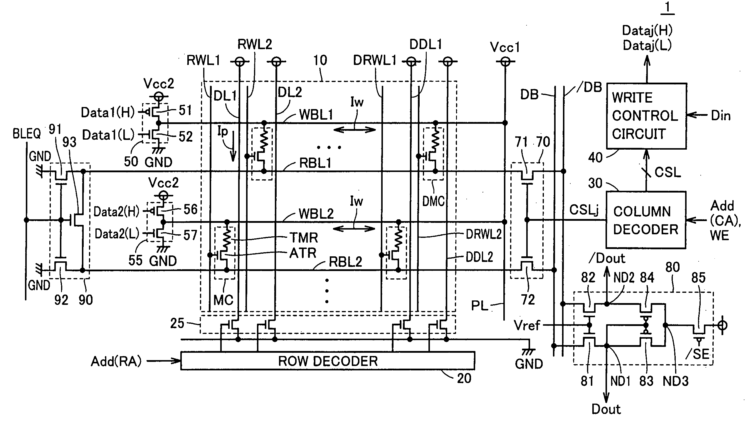
[0046]FIG. 1 is a circuit diagram representing an overall configuration of the MRAM in accordance with a first embodiment of the present invention.

[0047] Referring to FIG. 1, an MRAM 1 includes a memory array 10 including a plurality of MTJ memory cells MCs and a plurality of dummy MTJ memory cells DMCs arranged in a matrix of rows and columns, a row decoder 20, a digit line driver 25, a column decoder 30, a write control circuit 40, current drivers 50 and 55, a column selecting gate 70, a sense amplifier 80, and a precharge / equalize circuit 90.

[0048] The MRAM 1 further includes a plurality of read word lines RWL1, RWL2, . . . and a plurality of digit lines DL1, DL2, . . . provided corresponding to the rows of the memory cells, a plurality of dummy read word lines DRWL1, DRWL2, . . . and a plurality of dummy digit lines DDL1, DDL2, . . . also provided corresponding to the rows of the memory cells, a plurality of write bit lines WBL1, WBL2, . . . and a plur...

second embodiment

[0136] [Second Embodiment]

[0137] Though a voltage is always applied to common line PL in the first embodiment, in the second embodiment, a prescribed voltage is applied to common line PL only when the current driver is active.

[0138]FIG. 12 is a circuit diagram representing a configuration of a data write driver of the MRAM in accordance with the second embodiment.

[0139] Referring to FIG. 12, the data write driver of the MRAM has the configuration of data write driver in accordance with the first embodiment of FIG. 4, and additionally includes a signal output circuit 62 connected to common line PL. Further, to current drivers 50 and 55, not the power supply voltage Vcc2 but the power supply voltage Vcc1 is supplied.

[0140] Signal output circuit 62 receives the power supply voltage Vcc1 and the ground voltage GND, and generates and outputs to common line PL a φ signal. Here, the φ signal is at the L level represented by the ground voltage GND in the former half and at the H level re...

third embodiment

[0159] [Third Embodiment]

[0160] In the third embodiment, common line PL is shared by adjacent memory blocks

[0161]FIG. 14 is a circuit diagram representing a configuration of a data write driver of the MRAM in accordance with the third embodiment.

[0162] Referring to FIG. 14, in the MRAM in accordance with the third embodiment, a memory area including a plurality of MTJ memory cells MCs and a plurality of dummy MTJ memory cells DMCs arranged in a matrix of rows and columns is divided into at least one area, with each of the at least one area being divided into two blocks. In FIG. 14, blocks #1 and #2 of one such area are shown and the description will be given in the following with reference to the shown portions.

[0163] Block #1 includes current drivers 501 and 551, and corresponding write bit lines WBL11 and WBL21. Block #2 includes current drivers 511 and 561, and corresponding write bit lines WBL12 and WBL22. Current drivers 501, 551, 511 and 561 all receive power supply voltage...


PUM


Abstract

First and second current drivers are connected to one end of corresponding first and second write bit lines, respectively, and the first and second write bit lines are directly connected, at the other end, to a common line. The first and second current drivers receive a first power supply voltage and the ground voltage, while the common line receives a second power supply voltage higher than the ground voltage and lower than the first power supply voltage. The first and second current drivers cause a current for data writing to flow in a first direction based on a voltage difference between the first power supply voltage and the second power supply voltage, and cause a current for data writing to flow in a second direction based on a voltage difference between the second power supply voltage and the ground voltage.

Description

BACKGROUND OF THE INVENTION [0001] 1. Field of the Invention [0002] The present invention relates to a semiconductor memory device and, particularly, to a semiconductor memory device including a current driver that causes bi-directional current to flow through a data write line to write data into a memory cell. [0003] 2. Description of the Background Art [0004] An MRAM (Magnetic Random Access Memory) has been attracting attention as a non-volatile memory device with low power consumption. An MRAM is a memory device in which non-volatile data storage is realized by using a plurality of thin film magnetic bodies and each of the thin film magnetic bodies can be accessed at random. [0005] Recently, it has been reported that MRAM performance can remarkably be improved by using a thin film magnetic body utilizing magnetic tunnel junction (MTJ) as a memory cell. MRAMs including memory cells having the magnetic tunnel junction are disclosed in “A 10 ns Read and Write Non-Volatile Memory Arr...

Claims


Application Information

Patent Timeline
IPC IPC(8): G11C11/15G11C5/00G11C11/16
CPCG11C11/16
Inventor HIDAKA, HIDETO
Owner RENESAS ELECTRONICS CORP
Why Eureka
Try Eureka