Hydrogen assisted HDP-CVD deposition process for aggressive gap-fill technology

a technology of cvd film and hdp, which is applied in the field of manufacturing integrated circuits, can solve the problems of limiting the aspect ratio of gaps that hdp-cvd films are able to fill, affecting the efficiency of cvd film deposition, and difficult to fill high aspect ratio gaps using conventional cvd methods, etc., and achieves the effect of improving the gap-filling capability

Inactive Publication Date: 2005-01-13
APPLIED MATERIALS INC
View PDF99 Cites 14 Cited by
  • Summary
  • Abstract
  • Description
  • Claims
  • Application Information

AI Technical Summary

Benefits of technology

Embodiments of the present invention pertain to methods of depositing silicon oxide films using HDP-CVD deposition techniques. These embodiments enable improved gap-fill capabilities as compared to some other known HDP-CVD silicon oxide deposition techniques and are particularly useful for the manufacture of integrated circuits having minimum feature sizes of 0.10 microns or less.
According to one embodiment of the invention, a silicon oxide layer is formed over a substrate having a trench formed between adjacent raised surfaces in a multi-step process that includes depositing a first portion of layer over the substrate and within the trench by forming a high density plasma process that has simultaneous deposition and sputtering components from a first process gas comprising a silicon source, an oxygen source and molecular hydrogen with higher D / S ratio of 10-20, and thereafter, depositing a second portion of the silicon oxide layer over the substrate and within the trench by forming a high density plasma process that has simultaneous deposition and sputtering components from a second process gas comprising a silicon source, an oxygen source and molecular hydrogen with lower D / S ratio of 3-10. In one specific embodiment, the first portion of the silicon oxide layer reduces the height of the trench by 30-65 percent and the second portion of the oxide layer completes the filling of the trench.
According to another embodiment of the invention, a silicon oxide layer is formed over a substrate having a trench formed between adjacent raised surfaces in a multi-step process that includes depositing a first portion of layer over the substrate and within the trench by forming a high density plasma process that has simultaneous deposition and sputtering components from a first process gas comprising a silicon source, an oxygen source and helium and, thereafter, depositing a second portion of the silicon oxide layer over the substrate and within the trench by forming a high density plasma process that has simultaneous deposition and sputtering components from a second process gas comprising a silicon source, an oxygen source and molecular hydrogen. In one specific embodiment, the first portion of the silicon oxide layer reduces the height of the trench by 10-50 percent and the second portion of the oxide layer completes the filling of the trench.

Problems solved by technology

One persistent challenge faced by semiconductor manufacturers in the design and fabrication of such densely packed integrated circuits is the desire to prevent spurious interactions between circuit elements.
High aspect ratio gaps are difficult to fill using conventional CVD methods.
Semiconductor manufacturers have found out, however, that there is a practical limit to the aspect ratio of gaps that HDP-CVD films are able to fill.
It has been reported that when such a process is used to fill certain narrow-width, high aspect ratio gaps, the sputtering caused by argon in the process gas may hamper the gap-fill efforts.
This in turn, may result in the formation of a void in the gap if the upper areas of regrowth join before the gap is completely filled.
The '150 patent does not disclose specific details about what gaseous sources may be used to supply the hydrogen or how much hydrogen should be added.

Method used


Image

  • Hydrogen assisted HDP-CVD deposition process for aggressive gap-fill technology
  • Hydrogen assisted HDP-CVD deposition process for aggressive gap-fill technology
  • Hydrogen assisted HDP-CVD deposition process for aggressive gap-fill technology

Examples


Embodiment Construction

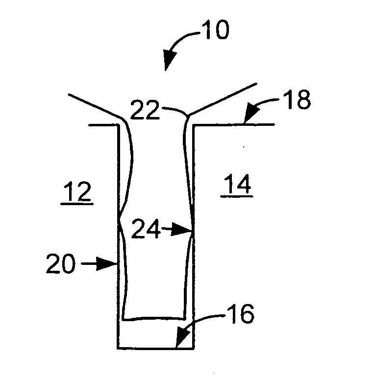
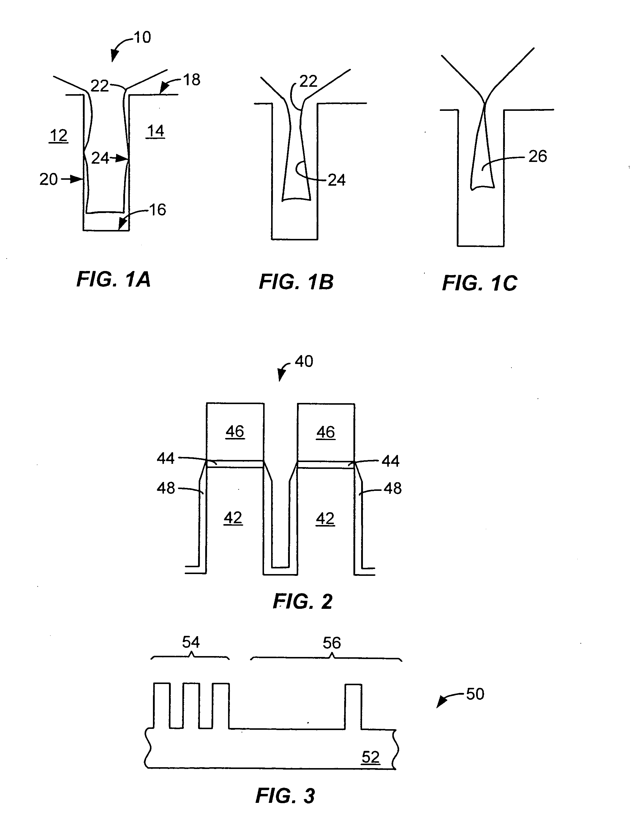
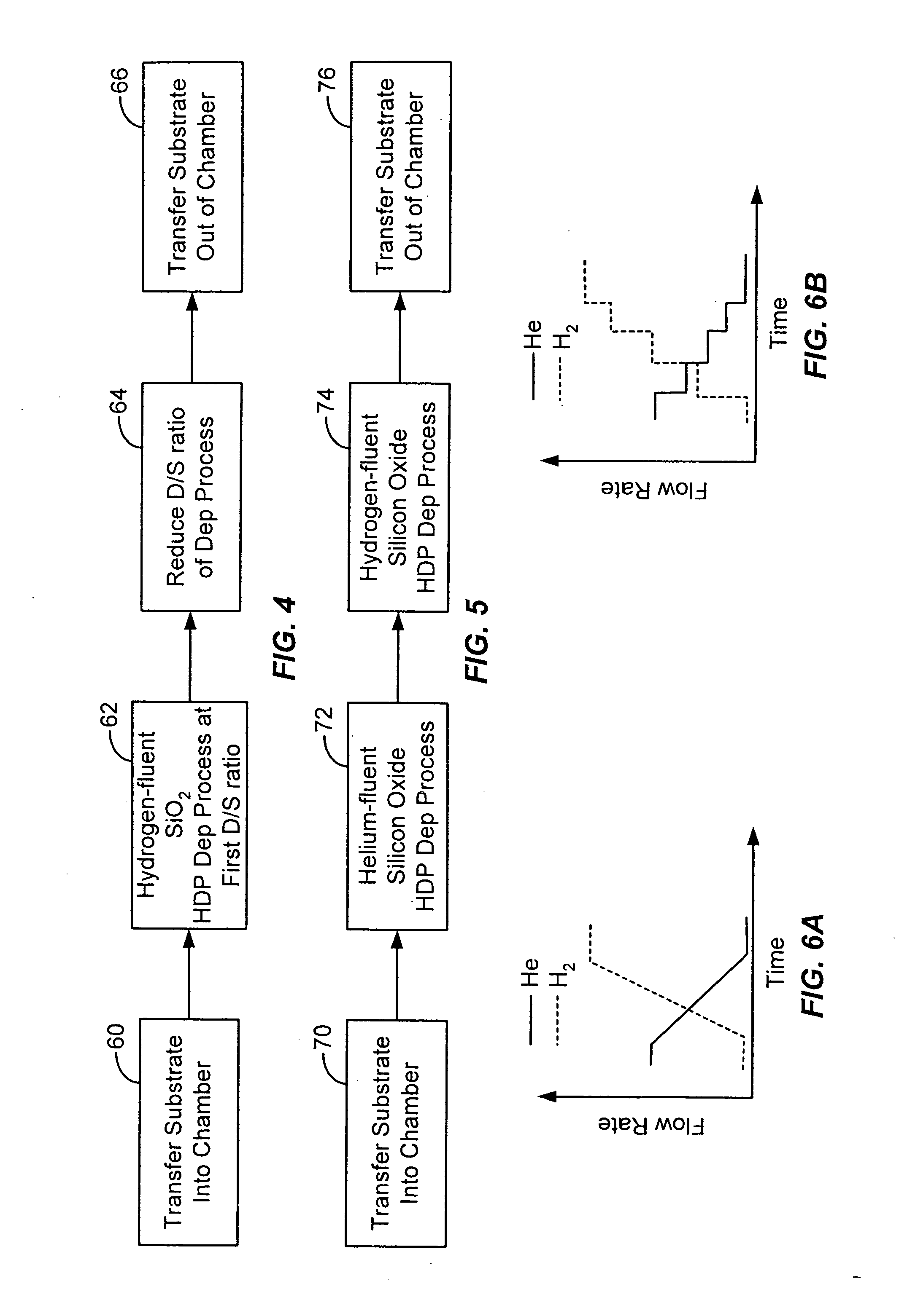
Embodiments of the invention are directed towards a method of depositing a silica glass layer to fill a gap in a surface of a substrate using a high density plasma CVD process. Silica glass films deposited according to the techniques of the invention have excellent gap-fill capabilities and are able to fill high aspect ratio gaps encountered in, for example, silicon trench isolation structures. Films deposited by the method of the invention are suitable for use in the fabrication of a variety of integrated circuits, and are particularly useful in the fabrication of integrated circuits having minimum feature sizes of 0.13 microns or less.

As used herein, a high density plasma process is a plasma CVD process that includes simultaneous deposition and sputtering components and that employs a plasma having an ion density on the order of 1×10¹¹ ions / cm3 or greater. The relative levels of the combined deposition and sputtering characteristics of the high-density plasma may depend on fact...


PUM

PropertyMeasurementUnit
feature sizesaaaaaaaaaa
ion densityaaaaaaaaaa

Abstract

A method of depositing a silicon oxide layer over a substrate having a trench formed between adjacent raised surfaces. In one embodiment the silicon oxide layer is formed in a multistep process that includes depositing a first portion of layer over the substrate and within the trench by forming a high density plasma process that has simultaneous deposition and sputtering components from a first process gas comprising a silicon source, an oxygen source and helium and / or molecular hydrogen with highD / S ratio, for example, 10-20 and, thereafter, depositing a second portion of the silicon oxide layer over the substrate and within the trench by forming a high density plasma process that has simultaneous deposition and sputtering components from a second process gas comprising a silicon source, an oxygen source and molecular hydrogen with a lowerD / S ratio of, for example, 3-10.

Description

BACKGROUND OF THE INVENTION The present invention relates to the manufacture of integrated circuits. More specifically, the invention relates to an improved method of depositing silicon oxide layers for use as a dielectric material in such integrated circuits. One of the primary steps in the fabrication of modern semiconductor devices is the formation of a film, such as a silicon oxide, on a semiconductor substrate. Silicon oxide is widely used as an insulating layer in the manufacture of semiconductor devices. As is well known, a silicon oxide film can be deposited by thermal chemical vapor deposition (CVD) or a plasma-enhanced chemical vapor deposition (PECVD) processes. In a conventional thermal CVD process, reactive gases are supplied to the substrate surface where heat-induced chemical reactions (homogeneous or heterogeneous) take place to produce a desired film. In a conventional plasma process, a controlled plasma is formed to decompose and / or energize reactive species to p...

Claims


Application Information

Patent Timeline
Patent Type & Authority Applications(United States)
IPC IPC(8): C23C16/04C23C16/40C23C16/44C23C16/455H01L21/316
CPCC23C16/045C23C16/402C23C16/45523H01L21/31612H01L21/02164H01L21/02211H01L21/02274H01J37/321
Inventor KAPOOR, BIKRAMKARIM, M. ZIAULWANG, ANCHUAN
Owner APPLIED MATERIALS INC
Why Eureka
Try Eureka